







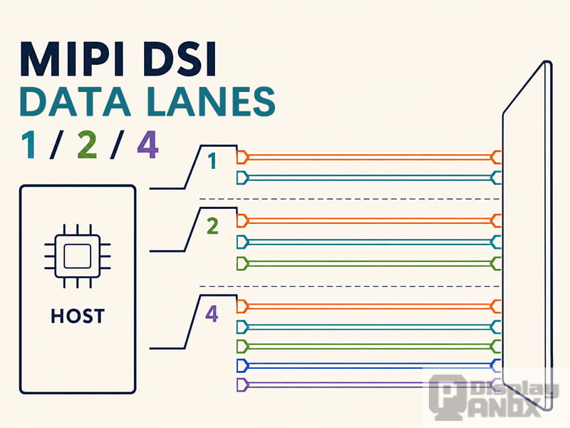
A conventional MIPI DSI display using a forwarded-clock D-PHY interface needs at least one clock lane and one data lane. Because every lane is a differential pair, the minimum physical connection consists of two differential pairs:
- One clock pair: CLK+ and CLK−
- One data pair: D0+ and D0−
A common single-link MIPI DSI interface can use up to four data lanes: D0, D1, D2, and D3. Commercial display modules most often use one, two, or four data lanes, although three-lane implementations also exist.
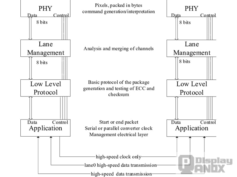
MIPI DSI interface architecture with one differential clock lane and four differential data lanes. Source: Yeming Liu and Chengyue He, A Design of MIPI DSI Interface for LCD Display Driver, CC BY 3.0.
The minimum number of data lanes depends mainly on resolution, refresh rate, pixel format, display timing, and the maximum lane rate supported by both the host processor and the display driver IC. The physical size of the screen has much less influence than the amount of pixel data transmitted every second.
What Is a MIPI DSI Data Lane?
MIPI DSI is a high-speed serial interface designed to connect a host processor to a display module. It is widely used in smartphones, tablets, wearables, automotive displays, embedded terminals, and AR/VR devices because it provides high bandwidth with fewer signal pins than a parallel display interface. The MIPI Alliance describes DSI as a high-performance, low-power, and low-EMI display interface.
In a conventional forwarded-clock D-PHY link, the clock lane provides timing for the high-speed transmission, while the data lanes carry image data, display commands, and protocol packets. Each additional data lane increases the total available bandwidth.
A four-lane link does not automatically improve image quality. It divides the same display stream across more lanes, reducing the required data rate on each individual lane.
This article focuses on the conventional MIPI DSI over D-PHY interface found on most commercial LCD, AMOLED, OLED, and Micro OLED modules. MIPI C-PHY uses three-wire trios with an embedded clock and follows a different physical structure.
Is One MIPI DSI Data Lane Enough?
One data lane can be sufficient for many small and medium-resolution displays. The answer depends on three main parameters:
- Pixel resolution
- Refresh rate
- Bits transmitted per pixel
The per-lane speed also matters. Many embedded MIPI DSI systems operate at several hundred megabits per second to around 1.5 Gbps per lane. D-PHY v1.2 increased the supported rate to 2.5 Gbps per lane, while newer D-PHY revisions can operate considerably faster. However, the usable rate in a real product is limited by the host controller, panel driver IC, PCB layout, connector, FPC, and signal-integrity margin—not merely by the theoretical D-PHY maximum. The MIPI D-PHY specification overview explains how the physical layer scales through one or more high-speed data lanes.
A low-resolution display can therefore work comfortably with one lane, while a high-resolution or high-refresh display may require two or four lanes.
How to Calculate the Required MIPI DSI Bandwidth
A quick estimate can be made from the active resolution:
Active pixel bandwidth = Width × Height × Refresh Rate × Bits per Pixel
For an RGB888 display, each pixel requires 24 bits. RGB666 uses 18 bits per pixel, while RGB565 uses 16 bits per pixel.
For example, the active pixel bandwidth of a 480 × 800 RGB888 display at 60 Hz is:
480 × 800 × 60 × 24 = 552,960,000 bit/s
The active image therefore requires approximately 553 Mbps before display timing and protocol overhead are considered.
For a more realistic Video Mode calculation, the horizontal and vertical blanking periods must also be included:
Pixel Clock = HTotal × VTotal × Refresh Rate
Required Link Rate = Pixel Clock × Bits per Pixel
Required Rate per Lane = Required Link Rate ÷ Number of Data Lanes
HTotal includes the active horizontal pixels, sync width, back porch, and front porch. VTotal includes the equivalent vertical values. The NXP MIPI DSI/CSI-2 application note uses this total-timing method when calculating pixel clock, total bandwidth, and data rate per lane.
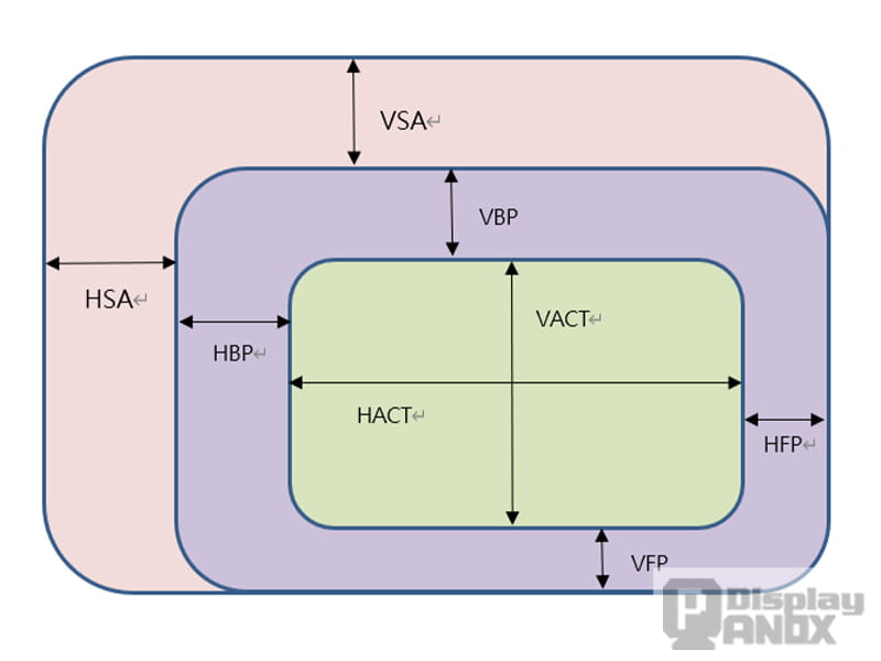
Active pixels and blanking intervals used to calculate MIPI DSI pixel clock.
Packet headers, checksums, lane transitions, controller restrictions, and engineering margin must also be considered. The exact overhead depends on the selected DSI mode and hardware implementation, so the panel and processor documentation should take priority over a universal percentage.
Typical Bandwidth and Lane Requirements
The following values use RGB888 at 60 Hz and count active pixel data only. They provide a useful first estimate but should not replace calculations based on the complete panel timing.
| Resolution | Active Bandwidth at 60 Hz | Typical Lane Configuration | Practical Assessment |
|---|---|---|---|
| 240 × 240 | 83 Mbps | 1 Lane | Easily supported |
| 320 × 480 | 221 Mbps | 1 Lane | Comfortable for most one-lane systems |
| 480 × 800 | 553 Mbps | 1 Lane | Usually practical when the lane supports sufficient headroom |
| 720 × 1280 | 1.33 Gbps | 2 Lanes | One lane leaves little or no timing margin on a 1.5 Gbps interface |
| 1080 × 1920 | 2.99 Gbps | 2 or 4 Lanes | Two lanes require a high per-lane rate; four lanes are more common |
| 1080 × 2400 | 3.73 Gbps | 4 Lanes | Four lanes are generally preferred |
| 1080 × 1920 at 120 Hz | 5.97 Gbps | 4 Lanes | Requires a high lane rate and may use compression |
These figures explain why a 480 × 800 display can often operate through D0 alone, while a 720p panel is normally configured with two data lanes.
For a 720 × 1280 RGB888 display at 60 Hz, the active stream already requires approximately 1.33 Gbps. A single 1.5 Gbps lane provides very little room for blanking and protocol overhead. Two lanes reduce the active payload to about 664 Mbps per lane, creating a much more practical operating range.
A 1080 × 1920 display requires approximately 2.99 Gbps for active RGB888 pixels at 60 Hz. With two lanes, each lane must carry about 1.49 Gbps before overhead is included. This can work when the panel and host support higher lane rates, but it is unsuitable for many systems limited to approximately 1.5 Gbps per lane. A four-lane configuration reduces the active load to about 747 Mbps per lane.
For 1080 × 2400 at 60 Hz, the active payload reaches approximately 3.73 Gbps. Four lanes reduce this to about 933 Mbps per lane, which is a practical configuration for many FHD+ mobile displays.
Common MIPI DSI Lane Configurations
Lane count varies by product design, but several patterns appear frequently in commercial displays.
| Display Application | Typical Resolution | Common Data Lane Count |
|---|---|---|
| Smartwatch or fitness band | 240 × 240 to 466 × 466 | 1 Lane |
| Smart home control panel | 320 × 480 | 1 Lane |
| Small handheld or instrument display | 480 × 800 | 1 or 2 Lanes |
| 720p handheld or mobile display | 720 × 1280 | 2 Lanes |
| Full HD mobile display | 1080 × 1920 | 2 or 4 Lanes |
| FHD+ smartphone display | 1080 × 2400 | 4 Lanes |
| Full HD high-refresh display | 1080p at 90–120 Hz | 4 Lanes |
| High-resolution tablet, VR, or Micro OLED | 1440p, 2K, or higher | 4 Lanes or dual-port MIPI |
These values are typical rather than mandatory. A compact Micro OLED can have a much higher resolution than a physically larger industrial LCD and may consequently require more data lanes. Screen diagonal alone is therefore a poor way to estimate the interface configuration.
Command Mode can also change the practical bandwidth requirement. A display controller with internal GRAM may store a frame and allow partial updates, reducing average link activity for static interfaces. Video Mode normally sends a continuous display stream and is more directly tied to the full pixel clock. Full-screen updates must still fit within the available link bandwidth.
How to Determine the Number of Data Lanes on a Display
The most reliable method is to check the display module specification and FPC pin assignment.
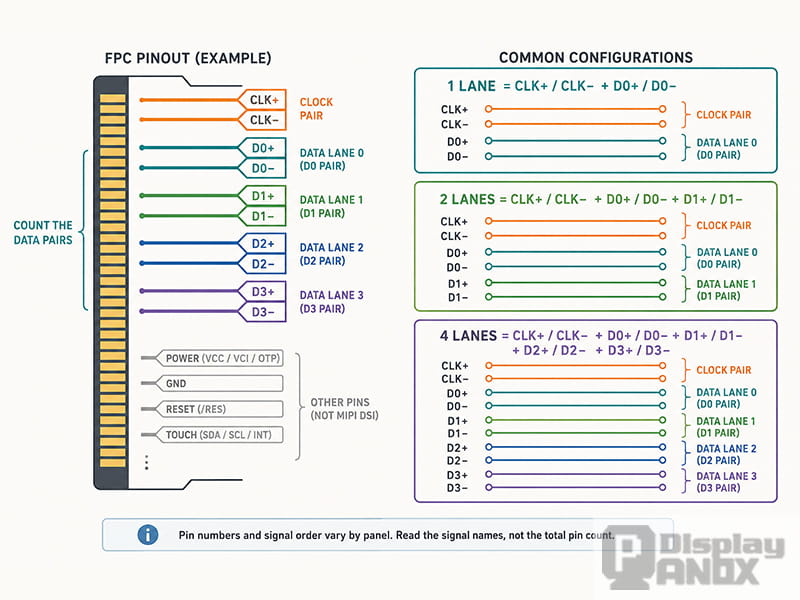
Example FPC pin assignments used to identify MIPI DSI clock and data lanes.
A one-lane module normally includes:
CLK± + D0±
A two-lane module normally includes:
CLK± + D0± + D1±
A four-lane module normally includes:
CLK± + D0± + D1± + D2± + D3±
The total number of FPC pins cannot identify the lane count by itself. A display connector may also include power rails, grounds, reset, tearing-effect synchronization, backlight control, touch signals, and identification pins. The pin names or schematic net labels must be checked for differential MIPI pairs.
The display driver IC datasheet is another important source. Some driver ICs can be configured for different lane counts through internal registers. Others have a fixed physical configuration. Even when the bare driver IC supports one, two, and four lanes, a particular display module may route only two of them through its FPC.
The initialization sequence should also be checked. The host DSI controller and the display driver must be configured for the same number of lanes. In Linux-based systems, the lane count may also appear in the display panel node or DSI host configuration.
Can Resolution Be Used to Estimate the Lane Count?
Resolution can provide a rough first estimate:
- Below 480p, one lane is often sufficient.
- Around 720p, two lanes are common.
- Full HD panels may use two or four lanes.
- FHD+, high-refresh, and higher-resolution panels generally use four lanes.
This estimate becomes unreliable when refresh rate, color format, blanking timing, or per-lane speed changes. A 1080p panel operating at 30 Hz requires only half the active bandwidth of the same panel at 60 Hz. A 120 Hz panel requires twice the active bandwidth.
RGB565 also needs one-third less active bandwidth than RGB888:
16 bpp ÷ 24 bpp = 66.7%
Display Stream Compression can further reduce the required link rate when supported by the complete display pipeline. The host, DSI controller, driver IC, and panel must all support the selected compression method.
Resolution is therefore useful for estimating a likely configuration, but it cannot confirm the actual lane count.
Can a Two-Lane or Four-Lane Display Run with One Lane?
Only when the display driver IC and the completed display module support that configuration.
A processor with one DSI data lane cannot automatically drive a two-lane panel by connecting D0 and leaving D1 unused. The panel must support one-lane operation, the required lane must be physically routed through the FPC, and the initialization sequence must configure the panel accordingly.
Grounding an unused data lane does not convert a fixed two-lane display into a one-lane display. An unsupported lane configuration usually results in a black screen, corrupted image, unstable synchronization, or failure during initialization.
The same rule applies when changing a four-lane panel to two lanes. Register-level support in the driver IC is only one requirement; the panel timing, module routing, host bandwidth, and initialization code must also match.
Why Not Use Four Data Lanes for Every Display?
Four lanes provide more total bandwidth at the same per-lane rate, but they also require more high-speed pins, additional differential routing, a larger connector allocation, and more complex layout control.
Using fewer lanes can simplify compact wearable and embedded designs. Using more lanes can lower the required rate on each lane, which may improve signal margin and reduce the difficulty of running a single differential pair at an extremely high frequency.
Power and EMI behavior must be evaluated for the complete system. Fewer active lanes do not always guarantee lower total power, especially if each lane must operate much faster. The practical objective is to select the lowest lane count that still provides sufficient bandwidth, timing margin, and compatibility.
A Practical MIPI DSI Lane Selection Process
A reliable lane decision should follow the complete display signal path:
- Obtain the panel’s active resolution, full horizontal and vertical timing, refresh rate, and pixel format.
- Calculate the pixel clock using HTotal × VTotal × refresh rate.
- Multiply the pixel clock by the number of bits per pixel.
- Divide the result by the proposed number of data lanes.
- Include the margin required by the DSI mode, packet structure, host controller, and panel documentation.
- Compare the result with the minimum and maximum lane rates supported by both the host and display.
- Confirm that the selected lane count is available on the processor, driver IC, display FPC, and initialization code.
At Panox Display, MIPI panel selection begins with the host processor and the complete display timing rather than screen size alone. The processor model, available DSI lanes, maximum lane rate, resolution, refresh rate, pixel format, operating mode, and FPC definition should all be confirmed before a panel is approved for a project. The Panox Display MIPI DSI interface guide provides additional information about the protocol, physical layer, and display integration process.
Conclusion
For a conventional forwarded-clock MIPI DSI D-PHY display, the minimum interface consists of one clock differential pair and one data differential pair:
CLK± + D0±
One data lane is often enough for low-resolution displays such as 240 × 240, 320 × 480, and many 480 × 800 modules. A 720p display normally uses two lanes, while Full HD, FHD+, and high-refresh panels commonly use two or four lanes. Very high-resolution displays may use four lanes, higher D-PHY rates, compression, or two separate MIPI DSI links.
Lane count should never be selected from resolution alone. The final decision must account for complete display timing, bits per pixel, refresh rate, DSI operating mode, per-lane speed, host limitations, driver IC support, and the actual FPC routing.
Learn more: MIPI DSI PCB Layout Guidelines for Reliable Display Interfaces