







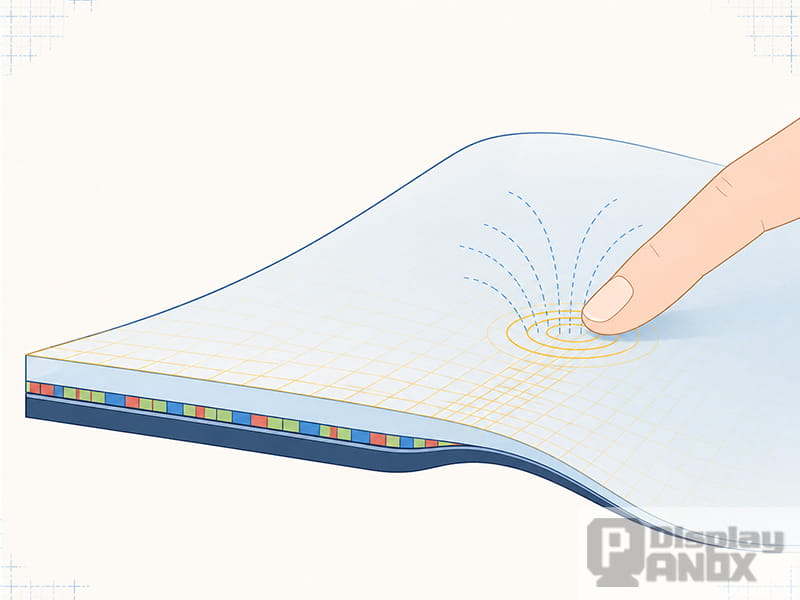
OLED displays are naturally thin, lightweight and capable of supporting curved, foldable and rollable designs. Touch input, however, adds another functional system to the display stack. The location of the touch sensor affects the total module thickness, optical performance, bending reliability, manufacturing yield and cost.
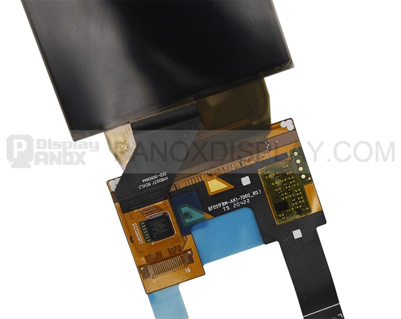
5.1 inch Flexible OLED On-Cell PACP For Cellphone
Touch integration has gradually moved from a separate panel attached above the display to sensors built directly on or inside the OLED panel. Four structures are commonly discussed: Out-Cell, On-Cell, In-Cell and Hybrid-Cell. Among them, On-Cell has become a mainstream OLED touch screen technology because it offers a practical balance between integration and manufacturability.
An On-Cell display is not necessarily the thinnest possible touch architecture. Full In-Cell integration can go further. On-Cell succeeds because it removes much of the thickness and optical loss associated with an external touch panel without introducing all the process complexity of embedding touch electrodes inside the OLED pixel structure.
How Touch Became Part of the OLED Display Stack
Early touchscreen products usually treated the display and touch panel as separate components. A completed touch sensor was laminated above the display with optical adhesive. This approach remains useful because it is mature, reliable and relatively easy to customize, but the additional films, adhesives and optical interfaces make the complete module thicker and heavier.
That trade-off became more important as OLED displays moved into smartphones, smartwatches and flexible devices. A flexible OLED can be extremely thin, but part of that advantage is lost when a separate, relatively stiff touch panel is attached above it. Additional layers can also increase bending stress, internal reflections and the number of interfaces that must be controlled during bonding.
On-Cell integration moves the touch sensor onto the OLED panel itself. In a flexible OLED, the touch electrodes are normally formed above the thin-film encapsulation layer, or TFE. The TFE protects the moisture-sensitive OLED materials while providing a surface on which the touch sensor can be patterned.
The transmitting and receiving electrodes can be arranged in two conductive layers separated by a dielectric layer. They can also be patterned in one plane, with bridge structures added where the row and column electrodes cross. The exact structure varies by panel maker, touch controller and display size, but the design principle remains the same: the touch sensor becomes part of the OLED panel rather than a completely separate overlay.
Out-Cell vs On-Cell vs In-Cell vs Hybrid-Cell
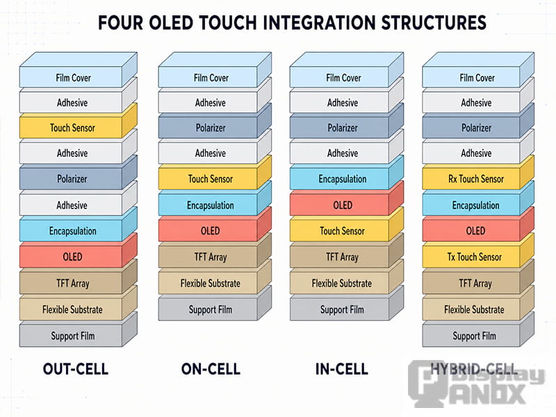
Out-Cell, On-Cell, In-Cell and Hybrid-Cell OLED Touch Structures
The four architectures are mainly distinguished by the position of the touch electrodes.
| Touch architecture | Sensor position | Main strengths | Main limitations |
|---|---|---|---|
| Out-Cell | A separate touch panel laminated above the display | Mature process, low technical risk, good yield, flexible customization and established supply chain | Thicker and heavier module, more optical interfaces and reduced bending performance |
| On-Cell | Touch electrodes formed on the OLED encapsulation layer | Thin and lightweight structure, good optical performance, suitable for flexible OLED and practical for volume production | Display noise, parasitic capacitance, floating-ground behavior and possible viewing-angle effects require careful design |
| In-Cell | Touch-sensing functions integrated inside the display cell or pixel structure | Highest integration, very thin stack and a short optical path | Complex fabrication, display-touch coordination, higher process risk and challenging noise control |
| Hybrid-Cell | Part of the touch system inside the display and part on the encapsulation layer | Balances integration with signal accessibility | Additional routing, larger side fan-out areas and more complicated manufacturing |
Out-Cell touch
Out-Cell is also called add-on, external or discrete touch. A separate touch panel is attached above the display module with optical adhesive. Common constructions include Film-Film, Film2, double-sided ITO and single-layer ITO with bridge structures.
Its advantages are straightforward. The process is mature, touch panels can be produced and tested independently, and display suppliers can combine one panel with different touch and cover-lens designs. Yields and long-term reliability are generally well understood.
The disadvantages come from the additional stack. A typical Out-Cell OLED module may include a cover lens, adhesive, touch sensor, another adhesive layer, polarizer, encapsulation, OLED layers, TFT backplane, flexible substrate and support film. The separate touch panel increases thickness and weight, while every additional interface can affect reflectance, transmission and flexibility.
Out-Cell remains useful when customization, repairability or a low-risk supply chain is more important than minimum thickness. It is less attractive for foldable displays and other products where the mechanical stack must bend repeatedly.
On-Cell touch
In an OLED On-Cell structure, the touch sensor is deposited or patterned above the OLED encapsulation layer. The sensor remains outside the active pixel and TFT structures, but it is already part of the display panel.
This position explains the main advantage of On-Cell. It removes the need for a complete external touch panel while keeping the touch process relatively separate from the most sensitive OLED fabrication steps. The resulting module can be thinner and lighter than an Out-Cell assembly without requiring touch electrodes to be fully embedded in the pixel structure.
Optical performance also benefits from the reduced number of separate films and adhesive interfaces. The touch pattern can use transparent conductive materials or fine metal-mesh electrodes aligned with the OLED pixel openings. A carefully designed pattern limits obstruction of emitted light and helps maintain image quality.
On-Cell still requires a cover lens or cover glass. Integrated touch removes the separate sensor panel; it does not remove the need for surface protection, sealing, coatings or the mechanical front structure.
In-Cell touch
In-Cell moves the touch-sensing function into the display cell. Depending on the panel architecture, touch may use dedicated electrodes inside the display or share parts of the display electrode structure.
This is the most highly integrated approach. With fewer separate functional layers above the pixels, In-Cell can offer a very thin module and excellent optical transmission. It can also support compact routing and narrow mechanical designs when the display and touch functions are coordinated through an integrated driver architecture.
The manufacturing challenge is much greater. Touch electrodes must coexist with TFT switching, pixel-driving signals and OLED emission without creating visible defects or unacceptable electrical interference. Display and touch scanning may need to be synchronized, and specialized driver ICs are often required.
Introducing additional patterns into the display cell can also affect process yield. A defect is no longer limited to an independently replaceable touch panel; it may affect the entire OLED panel. Parasitic capacitance and display noise are particularly difficult because the touch sensor sits close to high-frequency display-driving signals.
An In-Cell display can therefore achieve a higher level of integration, but that does not automatically make it the best choice for every product.
Hybrid-Cell touch
Hybrid-Cell divides the touch function between different parts of the panel. One common arrangement places the transmitting electrodes inside the display structure and the receiving electrodes on the OLED encapsulation layer.
This design can reduce the number of external sensor layers while keeping the receiving electrodes farther from some display-related interference. It occupies a middle position between On-Cell and full In-Cell integration.
The compromise introduces its own limitations. Internal transmitting electrodes may require additional fan-out routing along the left and right sides of the panel. That routing can occupy valuable border space and work against narrow-bezel designs. The process is also more complicated than a conventional On-Cell structure, which has limited the use of Hybrid-Cell to selected products.
Why On-Cell Became the Mainstream OLED Touch Solution
The success of On-Cell comes from several advantages working together rather than one dramatic performance difference.
First, it preserves much of the thin and lightweight character of OLED. A separate touch film and some associated adhesive layers can be removed, producing a cleaner front stack. This matters in smartphones, wearables and handheld products, where display thickness competes directly with the battery, enclosure and other electronics.
Second, On-Cell is a strong mechanical match for flexible OLED. Removing a discrete touch panel reduces the number of layers that must bend together. A thinner stack generally produces lower strain at a given bending radius, although the final reliability still depends on the electrode material, encapsulation, adhesives, cover layer, neutral-plane design and FPC routing.
Third, the touch process remains above the OLED encapsulation instead of being inserted deeply into the pixel fabrication sequence. This makes On-Cell easier to manufacture than full In-Cell touch and reduces the risk of disturbing OLED evaporation, TFT fabrication or pixel yield.
Fourth, it supports the projected capacitive touch performance expected from modern electronics. An On-Cell sensor can use a Tx-Rx mutual-capacitance matrix to provide accurate multi-touch, gestures and a responsive user interface. The architecture is therefore thin enough for premium products while remaining practical enough for volume production.
Finally, On-Cell offers a useful supply-chain balance. Display makers can provide an OLED panel with integrated touch while product developers retain control over the cover glass, optical bonding, touch firmware, enclosure and host electronics. This is one reason On-Cell OLED modules are available across wearables, mobile displays, handheld terminals and larger interactive devices.
From Panox Display’s perspective, On-Cell is often the practical starting point when a project requires integrated PCAP touch, a slim module and reasonable development risk. A module such as the 5.99-inch flexible OLED On-Cell display illustrates how high-resolution AMOLED, flexible construction and integrated touch can be supplied as one display platform.
How Capacitive Touch Detection Works
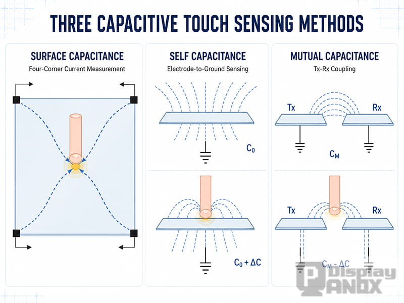
Surface, Self and Mutual Capacitive Touch Sensing
Most modern OLED touch displays use projected capacitive sensing. The basic idea is to detect a small change in an electric field when a conductive object, normally a finger, approaches the sensor.
The original development of capacitive touch includes three important mechanisms: surface capacitance, self-capacitance and mutual capacitance. Their sensing principles and electrode structures are different.
Surface-capacitive touch
A surface-capacitive panel uses a single conductive layer. An AC voltage is applied through electrodes positioned at the corners, creating an electric field across the surface.
When a finger touches the panel, it draws a small current from the conductive layer. The controller compares the current measured at the four corners and calculates the touch coordinate.
The structure is durable and relatively simple, but its resolution is limited and it does not provide the true multi-touch performance expected from smartphones and tablets. Surface-capacitive touch is therefore more commonly associated with large, simple information terminals than modern OLED mobile devices.
Self-capacitive touch
Self-capacitance measures the capacitance between a sensing electrode and ground. Without a finger, the electrode has a baseline capacitance. When a finger approaches, the human body creates an additional coupling path to ground, increasing the measured capacitance.
Self-capacitive sensing can provide strong sensitivity and fast scanning. It works well for buttons, proximity functions and simple touch interfaces. Its main weakness appears when row and column electrodes are used to detect multiple touches.
Suppose two fingers touch an X-Y grid at two separate points. The controller detects two active rows and two active columns, but it may not know which row belongs to which column. Four coordinate combinations are possible, even though only two are real. The additional intersections are called ghost points.
This ambiguity makes a basic X-Y self-capacitance grid unsuitable for unrestricted multi-touch.
Mutual-capacitive touch
Mutual capacitance measures the coupling between a transmitting electrode, Tx, and a receiving electrode, Rx. A switching voltage is applied to Tx, and the controller measures the charge coupled into Rx.
When a finger approaches a Tx-Rx intersection, part of the electric field is diverted through the body. The measured coupling between Tx and Rx normally decreases. Because every crossing belongs to a specific transmitter-receiver pair, the controller can identify the touched node directly.
Mutual-capacitive sensing supports true multi-touch without the ghost-point ambiguity of a basic self-capacitance row-column grid. It is therefore the dominant sensing method in smartphones, tablets and many modern capacitive touch screen systems.
The trade-off is a larger number of sensing nodes. The controller must drive multiple Tx lines and read multiple Rx channels, which can increase scanning time, processing requirements and power consumption. Controller architecture, scan strategy and firmware determine how effectively those costs are managed.
Touch Electrode Structures and Equivalent Circuits
The sensing mechanism becomes easier to understand by comparing three common electrode layouts.
X-Y self-capacitance grid
In an X-Y grid, the horizontal and vertical electrodes are measured separately against ground. A finger increases the capacitance of one or more rows and columns.
The layout is simple and requires fewer controller channels than an individually wired sensor array. Its weakness is the ghost-point problem. With two simultaneous touches, the controller sees the active rows and columns but cannot always determine which intersections contain the actual fingers.
Electrically, each row or column behaves like an electrode with a capacitance to ground. The finger adds another parallel capacitance. Position is inferred by combining the active X and Y measurements rather than measuring each intersection independently.
Independent self-capacitance electrode array
Ghost points can be eliminated by dividing the touch surface into independent electrodes and connecting every electrode directly to the touch IC. Each electrode then represents a unique touch location.
This works with one sensing layer and removes the row-column ambiguity, but it creates a routing problem. Every electrode needs its own trace. As the panel becomes larger or the resolution increases, the number of traces and IC pins rises quickly.
The wiring can consume a large part of the panel border or require another conductive layer to move the traces away from the active area. For a high-resolution display, the routing and controller-channel requirements can become impractical.
Tx-Rx mutual-capacitance matrix
A mutual-capacitance matrix uses one group of electrodes as transmitters and another as receivers. The touch IC activates the Tx lines in sequence and measures the response on all Rx channels.
Every intersection forms a sensing node with a mutual capacitance between its Tx and Rx electrodes. A finger changes the measured coupling at that node. Since the coordinate is defined by a unique Tx-Rx pair, multiple fingers can be tracked without creating the same ghost-point pattern as a simple self-capacitance grid.
This matrix structure is the natural match for an On-Cell OLED touch sensor. It supports multi-touch while allowing the transparent electrodes or fine metal mesh to be distributed across the active display area.
Engineering Challenges in On-Cell OLED Touch
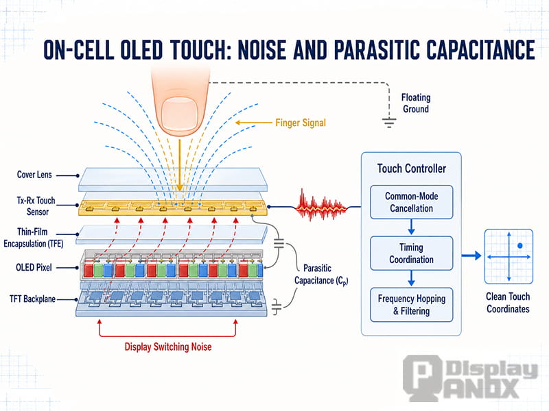
Display Noise and Parasitic Capacitance in On-Cell OLED Touch
On-Cell offers a strong overall balance, but placing the sensor close to the OLED introduces challenges that do not exist to the same degree in a separate external touch panel.
Viewing angle, color shift and electrode visibility
The touch electrodes sit in the optical path above the OLED pixels. If the conductive pattern is not coordinated with the pixel openings, it may reduce transmission, create non-uniformity or affect color at oblique viewing angles.
Transparent conductive materials help, but transparency is not the only requirement. Sheet resistance, line width, pattern pitch, reflectance and mechanical durability also matter. Metal-mesh structures may be aligned between pixel apertures to limit light obstruction, while ITO and other transparent conductors require a balance between conductivity and flexibility.
Pixel layout and touch-electrode design therefore need to be considered together. A pattern that works well on one OLED pixel arrangement may produce moiré, visibility or color-shift problems on another.
Display noise
An AMOLED panel contains many switching signals. TFT gates, source lines, power rails and pixel-driving waveforms can couple into the touch sensor. Because the On-Cell electrodes are close to the display, the background capacitance and common-mode noise can be much larger than the small signal created by a finger.
If the touch controller lacks sufficient input range or noise rejection, display interference can hide the touch signal or saturate the receiver. Practical systems may use differential sensing, common-mode cancellation, optimized scan timing, filtering and frequency hopping. Some designs coordinate touch scanning with display timing, while others use asynchronous noise-removal methods to avoid dependence on a fixed refresh rate.
Floating ground and parasitic capacitance
A mobile or wearable product is usually battery powered and does not have a fixed earth connection. Its electrical ground can therefore float relative to the user. The resulting body-to-device coupling changes with the enclosure, charging state, hand position and surrounding environment.
Parasitic capacitance from the display, FPC, cover lens, frame and nearby conductive components also changes the sensor baseline. These effects influence sensitivity and signal-to-noise ratio, particularly on larger panels.
Grounding strategy, shielding, electrode routing, touch-controller capability and calibration must be evaluated in the finished device rather than only on an exposed display sample.
Power and scan time
A high-resolution mutual-capacitance matrix contains many sensing nodes. Reading all of them at a high rate consumes time and power. A low scan rate can make the interface feel delayed, while aggressive scanning increases power consumption and may create more electromagnetic interference.
Touch controllers address this through region-based scanning, adaptive scan rates, noise-aware frequency selection and low-power wake-up modes. The correct balance depends on display size, refresh rate, expected gestures and battery requirements.
Flexible and foldable reliability
On-Cell is well suited to flexible OLED, but the name alone does not guarantee foldability. The electrode material must maintain conductivity after repeated bending, and the dielectric and bridge structures must resist cracking or delamination.
The complete mechanical stack matters. Cover films, optical adhesive, TFE, support layers, hinge geometry and FPC exit direction all influence strain. A reliable flexible OLED touch screen is therefore a system-level design rather than a flexible panel with an ordinary cover glass attached on top.
Choosing an On-Cell OLED Display for a Product
The touch structure should be evaluated together with the rest of the display system. Screen size, resolution, brightness and interface are only the starting points. The specification must also identify the touch controller, touch communication interface, number of supported touch points, cover-lens requirements, optical-bonding method, FPC layout, grounding recommendations and operating environment.
Glove operation, wet-touch behavior, stylus support, palm rejection and ESD requirements should be defined before the cover glass is finalized. A thicker cover lens or a large air gap may reduce sensitivity, while metal enclosures and poorly routed FPCs can introduce noise.
Flexible projects require additional mechanical information, including minimum bending radius, bend direction, number of cycles, whether the panel bends while powered and the position of the neutral mechanical plane. Panox Display’s overview of On-Cell display applications covers suitable module directions for wearables, handheld terminals, industrial interfaces and flexible devices.
The Future of Sensor Integration in OLED Displays
Touch is currently the most familiar non-display function integrated into an OLED panel, but it is unlikely to be the last.
A display occupies most of the front surface of a modern device and remains close to the user during operation. That makes it a natural platform for additional functions such as fingerprint sensing, ambient-light detection, temperature sensing, pressure detection and optical biometric sensing. Conductive structures around or within the display may also support communication or antenna-related functions.
Many of these ideas remain limited by cost, optical interference, electrical noise, process maturity or performance. Their adoption will depend on advances in materials, thin-film fabrication, sensor algorithms, power consumption and system integration.
The direction, however, is clear. As devices become thinner and front surfaces become more continuous, the OLED panel will take on more responsibilities beyond image generation.
Conclusion
On-Cell became a mainstream OLED touch screen technology because it occupies the most useful point between two extremes.
Out-Cell touch is mature and flexible to customize, but its separate sensor and adhesive layers add thickness, weight and mechanical stiffness. In-Cell can achieve the highest integration and thinnest optical stack, but it requires closer coordination between touch and display, more complex manufacturing and stronger noise control.
On-Cell removes the separate touch panel by forming the sensor on the OLED encapsulation layer. It preserves much of the optical and mechanical advantage of OLED while keeping the manufacturing process more practical than full In-Cell integration. Combined with a Tx-Rx mutual-capacitance matrix, it provides the multi-touch performance expected from modern smartphones, wearables, handheld terminals and flexible displays.
Its position as the mainstream option is therefore not based on one absolute performance record. It comes from a better overall balance of thickness, image quality, flexibility, touch performance, manufacturing yield, development risk and cost.