







MIPI interfaces are widely used in smartphones, tablets, industrial terminals, embedded computers, automotive electronics, cameras and compact display systems. However, “MIPI” is often treated as the name of one connector or one display interface. In reality, MIPI Alliance develops a family of interface specifications for different functions inside electronic devices.
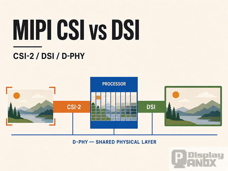
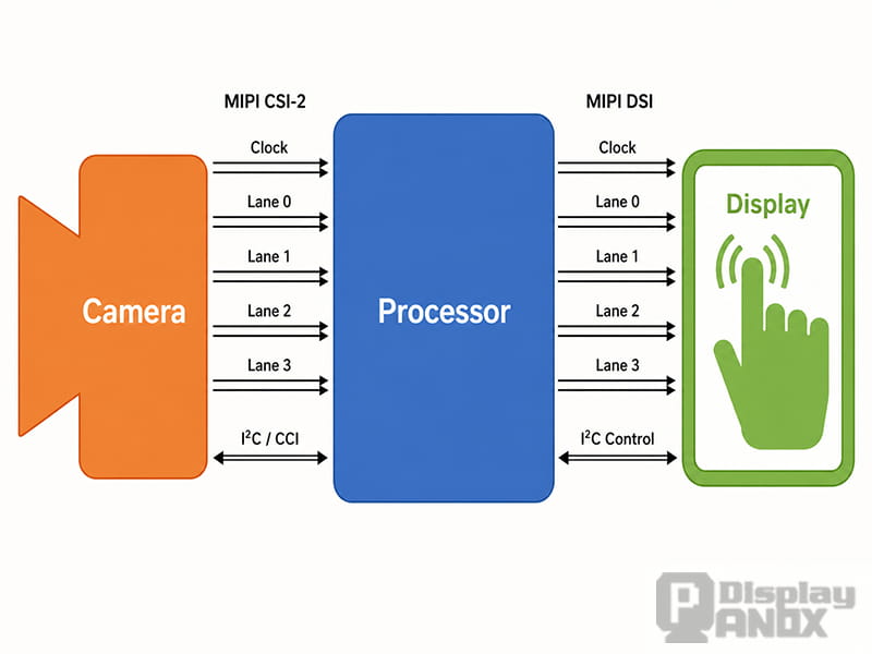
For imaging systems, three terms appear most often: MIPI CSI-2, MIPI DSI and MIPI D-PHY. CSI-2 usually carries image data from a camera sensor to a processor. DSI carries display data from a processor to a display panel. D-PHY defines the electrical signaling and lane behavior beneath these protocols.
A complete embedded imaging path may therefore contain both CSI-2 and DSI:
Image sensor → CSI-2 → processor and ISP → frame buffer → DSI → display panel
Understanding the difference between these layers makes interface selection, driver development and display troubleshooting much more straightforward.
What MIPI Means—and Why CSI-2, DSI and D-PHY Are Different
MIPI is not a single bus. It is an ecosystem of specifications covering cameras, displays, sensors, storage, chip-to-chip communication and other subsystem connections.
Within a typical camera and display system, CSI-2 and DSI define how information is organized and transported, while D-PHY defines how that information travels electrically across the PCB or flex cable.
| Term | Main role | Typical direction |
|---|---|---|
| MIPI CSI-2 | Camera and image-sensor data protocol | Image sensor to processor |
| MIPI DSI | Display command and pixel-data protocol | Host processor to display |
| MIPI D-PHY | Physical layer defining lanes, electrical states and link transitions | Used beneath CSI-2 or DSI |
| ISP | Image-processing hardware or pipeline | Processes captured sensor data |
The distinction matters because two devices using D-PHY are not automatically compatible. A CSI-2 transmitter and a DSI receiver may use similar differential lanes, but their packet types, control procedures and system roles are different. A direct wire connection cannot convert one protocol into the other.
Modern CSI-2 and DSI-2 specifications can also operate over other MIPI physical layers, including C-PHY and, for certain applications, A-PHY. D-PHY remains the most familiar implementation in compact embedded cameras and displays, so it is the main physical layer discussed here. The current capabilities of each interface family are described on the official MIPI CSI-2, MIPI DSI-2 and MIPI D-PHY pages.
MIPI CSI-2 vs DSI at a Glance
CSI-2 and DSI are often found in the same product, but they handle opposite sides of the imaging pipeline.
CSI-2: From the Camera Sensor to the Processor
A typical CSI-2 capture path is:
Image sensor → CSI-2 transmitter → D-PHY → CSI-2 receiver → ISP, DMA or memory
The sensor measures light and converts it into digital pixel samples. Its CSI-2 transmitter packages those samples into frames, lines and pixel payloads. The SoC receives the packets through a CSI-2 controller and then routes the data to an ISP, DMA engine or memory buffer.
Sensor configuration is usually handled through a separate control connection, commonly I²C-compatible CCI. CSI-2 carries the image stream; it is not normally responsible for programming exposure registers, gain settings or sensor operating modes.
DSI: From the Processor to the Display
A typical MIPI DSI display path is:
Application or UI → GPU → frame buffer → display controller → DSI host → D-PHY → display driver IC → panel pixels
The application and graphics engine produce an image in memory. The display controller reads that frame buffer, applies the required resolution, stride, timing and pixel format, and forwards the result to the DSI host. The DSI host then packages commands or pixel data for transmission to the panel.
Inside the display module, the display driver IC interprets the DSI traffic and drives the TFT LCD, OLED or other display technology. DSI is therefore more than a set of differential wires: it also includes command handling, pixel formats, video timing and panel operating modes.
Why CSI-2 and DSI Are Not Interchangeable
The same D-PHY hardware may sometimes be configurable for CSI-2 or DSI, but this is a capability of a specific SoC—not a general property of the protocols.
A CSI-2 camera port cannot directly drive a MIPI DSI display. Likewise, a DSI transmitter cannot directly receive a CSI-2 sensor stream. Conversion requires a controller, FPGA, SoC pipeline or dedicated bridge that terminates one protocol and generates the other.
How MIPI D-PHY Carries CSI-2 and DSI Traffic
D-PHY provides the electrical link used by many CSI-2 cameras and DSI displays. It combines high-speed differential transmission with low-power single-ended signaling on the same conductors.
Clock Lanes and Data Lanes
A conventional forwarded-clock D-PHY link contains one differential clock lane and one or more differential data lanes. Many embedded camera and display designs use one, two or four data lanes, although supported configurations depend on the host and peripheral.
A common two-lane MIPI DSI interface contains:
| Lane | Signals | Function |
|---|---|---|
| Clock lane | CLK_P and CLK_N | Forwards the high-speed link clock |
| Data lane 0 | D0_P and D0_N | Carries packet data and commonly supports turnaround |
| Data lane 1 | D1_P and D1_N | Adds data bandwidth |
“Two-lane MIPI” therefore means two data lanes, not two differential pairs in total. A traditional two-lane link has one clock pair and two data pairs—six high-speed signal conductors before ground, shielding and other panel connections are counted.
Reset, Tearing Effect output, touch I²C, power rails, backlight control and enable signals are not part of the D-PHY lane group, even when they appear on the same connector.
Payload bytes are distributed across the active data lanes and restored in order by the receiver. The lanes do not normally represent separate halves of an image or fixed groups of pixels.
Most current embedded panels still use a forwarded clock lane. Newer D-PHY revisions also define an optional embedded-clock mode, so the statement that every possible D-PHY link must have a separate clock lane is no longer universally true. The conventional clock-plus-data arrangement remains the most relevant configuration for common MIPI DSI display modules.
High-Speed and Low-Power Signaling
D-PHY switches between High-Speed and Low-Power electrical states according to the operation being performed.
| State | Electrical method | Typical role |
|---|---|---|
| High-Speed (HS) | Low-swing differential signaling | Pixel payloads and other high-throughput data |
| Low-Power (LP) | Single-ended signaling on the P and N conductors | Link control, initialization, escape communication and state changes |
| Ultra-Low Power State (ULPS) | Defined low-power lane state | Reduces interface power during extended idle periods |
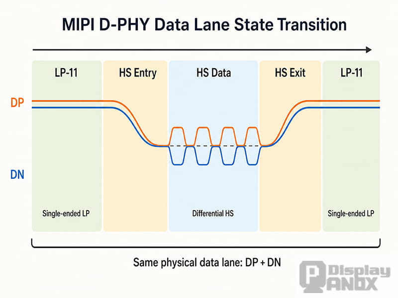
LP-11 is commonly used as the D-PHY Stop State. When high-speed transmission is required, the lane passes through a defined request and preparation sequence, enters HS operation, sends the payload, and then returns to the LP state. The transition timing must satisfy both the host and peripheral requirements.
ULPS is entered through a specified sequence. Observing LP-00 alone does not prove that a link has entered ULPS, because LP-00 may also appear during other D-PHY transitions.
The main direction of a DSI link is from the host to the display. However, DSI can support limited reverse communication through Bus Turnaround, typically using data lane 0 in Low-Power mode. This allows operations such as reading a panel ID, retrieving status or receiving an acknowledgement when the host and panel support them.
Most importantly, HS and LP must not be confused with DSI Command Mode and Video Mode. HS and LP describe D-PHY electrical states. Command Mode and Video Mode describe how DSI delivers content to the display. Commands may be transmitted through LP or HS, depending on the host, panel and command type, while a Video Mode link may enter LP during blanking intervals when supported.
How MIPI Packets Are Transmitted
CSI-2 and DSI define different data types, but both use packet-based transport.
Short packets are generally used for synchronization events, status information or commands with little or no payload. Long packets contain a header, a variable-length payload and a checksum. Pixel data is normally carried in long packets.
The packet header contains fields that identify the packet type and logical channel. Header ECC protects the header, while a CRC protects the payload of a long packet. These protections should not be described as one universal “MIPI ECC,” because they cover different parts of the transmission.
CSI-2 virtual channels can distinguish logical image streams, such as data from multiple sensors or multiple exposures, when the devices and receiver support that arrangement. DSI uses data types to distinguish commands, pixel formats and synchronization information.
Inside MIPI CSI-2: RAW Data and the ISP Pipeline
Many image sensors transmit Bayer RAW samples over CSI-2. RAW8, RAW10 and RAW12 describe the number of bits used for each pixel sample on the CSI-2 stream.
| Format | Sample depth | Common CSI-2 packing |
|---|---|---|
| RAW8 | 8 bits | One pixel per byte |
| RAW10 | 10 bits | Four pixels packed into five bytes |
| RAW12 | 12 bits | Two pixels packed into three bytes |
RAW10 packing illustrates an important point: the link does not send every 10-bit sample in a separate 16-bit word. Four 10-bit samples contain 40 bits, which fit into five bytes. RAW12 similarly packs two 12-bit samples into three bytes. NXP’s MIPI DSI/CSI-2 application note provides practical examples of CSI-2 pixel packing.
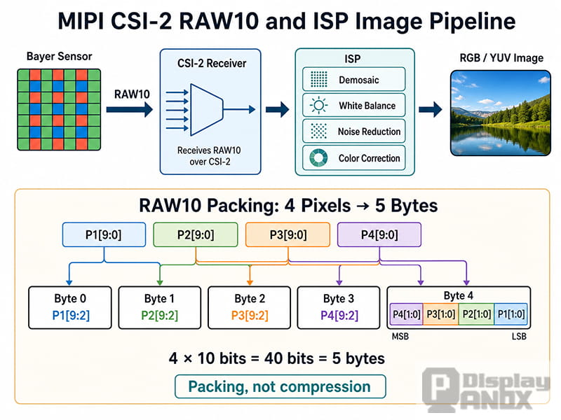
Packing is not the same as compression. Packing removes unused padding between samples, while compression applies a data-reduction method. CSI-2 can support separate compression techniques, but RAW10 packing itself is not a compressed image format.
After reception, an SoC may preserve the packed representation or expand each sample into a 16-bit memory word. Consequently, the memory stride and buffer size may be larger than the CSI-2 wire format suggests.
A higher RAW bit depth provides more quantization levels: RAW8 has 256 possible values, RAW10 has 1,024 and RAW12 has 4,096. It does not automatically guarantee higher dynamic range or better image quality. Sensor noise, full-well capacity, analog gain, ADC performance, exposure control, lens quality and ISP processing remain equally important.
What the ISP Does
Bayer RAW data is not normally ready for direct display. The sensor measures one color component at each photosite according to its color filter pattern. An Image Signal Processor converts those samples into a usable image.
Typical ISP operations include demosaicing, black-level correction, defective-pixel correction, white balance, color correction, noise reduction, tone mapping, HDR processing, sharpening and conversion to RGB or YUV.
CSI-2 transports the sensor data; the ISP processes it. The ISP does not “convert MIPI into RGB.” Some sensors contain an internal ISP and can output YUV or RGB directly, while others provide Bayer RAW data for processing inside the host SoC.
Inside MIPI DSI: From Frame Buffer to Display Panel
The display side begins with an image stored or generated inside the host. The display controller reads that image according to its resolution, stride and pixel format. The DSI host converts the output into DSI packets and sends them through D-PHY.
Common display pixel formats include RGB565, RGB666 and RGB888, although the exact formats depend on the host and panel driver IC. The DSI packet data type, host output format and panel pixel-format register must agree. A mismatch may produce incorrect colors, shifted pixels or a completely unusable image.
Before valid pixels can be displayed, the panel usually requires a defined sequence:
- Power rails must reach the required levels in the correct order.
- Reset must be asserted and released with the specified timing.
- Initialization commands must configure the display driver IC.
- Sleep Out and Display On commands must be issued at the correct stage.
- The DSI host must enter the required display mode with matching lane and timing settings.
Video Mode panels still require command-based initialization. The phrase “Video Mode does not use commands” is therefore incorrect.
For a deeper display-specific protocol description, the Panox Display complete MIPI DSI interface guide covers DCS commands, packet structure, Linux bring-up and related design considerations.
MIPI DSI Command Mode vs Video Mode
Command Mode and Video Mode describe two ways of supplying display content.
| Characteristic | Command Mode | Video Mode |
|---|---|---|
| Transfer method | Commands and pixel writes update the display | Host sends a timed pixel stream |
| Panel memory | Usually relies on display GRAM or frame memory | Often uses limited buffering and depends on host timing |
| Refresh behavior | Full or partial regions can be updated when required | Pixels are normally streamed every frame |
| Synchronization | TE can coordinate updates with panel scanning | Horizontal and vertical timing control the stream |
| Typical benefit | Partial updates and link idle time may reduce power | Direct, predictable continuous display output |
| Main requirement | Host must follow the panel’s command/update procedure | Host must continuously satisfy line and frame timing |
Command Mode is commonly used by panels with internal display memory. The host sends DCS commands and pixel data to update the entire frame or a selected rectangular region. The DSI link may remain idle between updates, and the panel can continue scanning its internal memory.
This can reduce data transfer and power in interfaces that change only part of the screen, but Command Mode is not simply a “still-image mode.” It can support animated interfaces and frequent updates when sufficient bandwidth is available.
The Tearing Effect signal is often used to coordinate Command Mode updates with the panel’s refresh cycle. Updating at the wrong time can create a visible boundary between old and new frame content.
Video Mode delivers a continuous, timing-dependent stream. The traditional DSI Video Mode options are Burst Mode, Non-Burst Mode with Sync Events and Non-Burst Mode with Sync Pulses. Burst Mode sends active pixel data at a higher instantaneous rate and may leave additional idle time. Non-Burst modes transmit data in a way that more closely represents the display timing.
Whether the link enters LP during blanking, uses a continuous clock or requires particular end-of-transmission behavior depends on the host and panel. These settings must come from the display driver IC documentation rather than a generic assumption.
Modern DSI-2 systems can support more adaptive or hybrid behavior, further reducing the value of treating Command Mode and Video Mode as rigid opposites.
MIPI DSI Lane Count and Bandwidth
Resolution alone does not determine whether a one-, two- or four-lane interface is required. Refresh rate, pixel format, blanking intervals, packet overhead and the maximum supported lane rate all affect the result.
For a basic Video Mode estimate:
Pixel clock = Htotal × Vtotal × frame rate
Minimum aggregate payload bandwidth = pixel clock × transmitted bits per pixel
Theoretical per-lane rate = aggregate bandwidth ÷ number of active data lanes
Htotal and Vtotal include active pixels, sync periods and front and back porches. The theoretical result is not a final hardware setting. DSI packet headers, CRC, transitions, blanking behavior, Burst or Non-Burst operation, PLL limitations and implementation margin must also be considered.
Increasing the lane count reduces the required data rate per lane, but it consumes additional pins and may not be supported by the panel. A two-lane panel cannot be assumed to operate as a four-lane panel, even if the display driver IC family supports both configurations.
The host’s pixel clock, D-PHY bit clock, byte clock and escape clock are related but not interchangeable. Treating MHz, pixel clock and lane Mbps as the same parameter is a frequent source of configuration errors.
Can MIPI CSI-2 and DSI Run at the Same Time?
CSI-2 camera capture and DSI display output can operate simultaneously when the SoC provides the necessary independent resources. This is common in camera preview systems, machine-vision terminals and video-monitoring products.
Simultaneous operation depends on more than the existence of two software drivers.
| Resource | What must be verified |
|---|---|
| Controllers | Independent CSI-2 receiver and DSI host blocks |
| Physical layers | Separate or concurrently usable RX and TX PHY resources |
| Pin multiplexing | Camera and display pins must not overlap |
| Clocks and PLLs | Both interfaces must have compatible clock sources |
| Power and reset domains | Enabling one block must not disable or reset the other |
| Data path | ISP, DMA, display controller and memory routes must be available |
| System bandwidth | Memory and internal buses must sustain capture and display traffic |
| Software | Drivers, device-tree resources and interrupts must not conflict |
Some SoCs provide independent CSI RX and DSI TX blocks and can run both at once. Others multiplex the same D-PHY, lane group, PLL or internal video port between CSI and DSI. In such cases, the hardware may allow only one function at a time.
A driver marked as enabled does not prove that the hardware path is valid. Clock handles, regulators, reset controls, PHY assignments, pin groups, interrupts and DMA resources must all be checked.
Common MIPI DSI Display Problems
A MIPI display problem may come from power, initialization, packet configuration, timing, memory bandwidth or PCB signal integrity. Starting with the PCB before validating the basic display pipeline often wastes time.
| Symptom | Likely causes | Priority checks |
|---|---|---|
| Panel remains dark | Missing power, reset error, backlight disabled, failed initialization | Rails, reset waveform, DCS sequence and required delays |
| Panel responds but shows no image | LP commands work, but HS stream or timing is wrong | Lane count, clock, Video Mode type and display controller output |
| Image is shifted or rolling | Incorrect active size, porch or line timing | HACT, VACT, HSA, HBP, HFP, VSA, VBP and VFP |
| Colors are incorrect | Pixel-format or byte-order mismatch | RGB565/666/888, RGB/BGR order, packet data type |
| Random lines or intermittent corruption | Marginal signal integrity, FIFO underrun or clock error | Error counters, memory bandwidth, lane rate and PCB routing |
| Flicker or freezing | Insufficient bandwidth, unstable PLL, LP/HS transition issue | Clocks, FIFO status, refresh rate and D-PHY timing |
| Visible tearing | Unsynchronized updates or buffer switching | TE configuration, VSync and double buffering |
1. Establish a Known Display Output
If the display driver IC provides an internal color-bar or test-pattern generator, enable it first. A correct internal pattern confirms that the panel glass, driver output and much of the power system are functioning. It does not prove that the DSI data path is correct, but it separates panel problems from host-stream problems.
2. Test the Frame Buffer with Simple Colors
Generate solid red, green, blue, white and black frames before testing a complex user interface. A gradient or pixel-coordinate pattern can expose incorrect stride, swapped color channels, active-area errors and pixel packing problems.
The frame-buffer resolution, memory stride and format must match the display controller configuration. Correct DSI electrical signaling cannot repair an incorrectly described source buffer.
3. Match the Panel Configuration Exactly
Confirm the lane count, lane mapping, P/N polarity, Command or Video Mode, Burst or Non-Burst setting, clock behavior, pixel format, per-lane data rate and complete horizontal and vertical timing.
Host, bridge and panel settings must agree. A configuration copied from a similar-resolution panel may still fail because the display driver IC, initialization sequence or blanking requirements are different.
4. Recheck Power, Reset and Initialization Timing
Many displays require delays after power-on, reset release, Sleep Out and other commands. Shortening these delays can produce inconsistent behavior in which the panel occasionally starts and occasionally remains blank.
A successful panel-ID read proves that some LP communication works. It does not prove that the HS pixel stream, lane configuration or display timing is correct.
5. Read the Controller Error Status
Check hardware registers and driver logs for Start-of-Transmission errors, synchronization errors, header ECC errors, payload CRC errors, timeouts, PLL unlocks, FIFO underruns and FIFO overflows.
These indicators help distinguish packet corruption from a display-controller or memory-throughput problem. A clean link with a persistent color error points more strongly toward pixel format or panel register configuration than PCB signal integrity.
6. Reduce the Data Rate as a Diagnostic Test
Temporarily lower the refresh rate, resolution or lane rate while keeping the configuration within panel limits. If the display becomes stable at a lower throughput, the original design may have insufficient bandwidth margin, unstable clocks or a signal-integrity problem.
This test identifies a direction for investigation; it is not a substitute for calculating the final lane rate.
7. Inspect the Physical Link
After configuration and bandwidth have been validated, inspect controlled differential impedance, intra-pair matching, lane-to-lane skew, return-path continuity, connector transitions, vias and the loading introduced by ESD protection devices.
Long flex cables, unsuitable common-mode chokes, excessive stubs and polarity or lane-order errors can prevent reliable HS operation even when LP commands still work. The Panox Display MIPI DSI PCB layout guidelines provide more detailed routing considerations, while the MIPI DSI display bring-up guide covers the full initialization and debugging sequence.
Choosing a MIPI DSI Display for a Real Product
A display cannot be selected by resolution and connector size alone. The complete interface contract must match the host platform.
| Category | Information to confirm |
|---|---|
| Image requirements | Resolution, refresh rate, pixel format, orientation and color depth |
| DSI configuration | Lane count, permitted lane rate, Command or Video Mode and clock behavior |
| Panel control | Display driver IC, initialization code, reset timing, TE and readback support |
| Electrical design | I/O voltage, power rails, backlight circuit, touch interface and ESD strategy |
| Mechanical integration | Active area, outline, connector, pinout, FPC direction and mounting constraints |
| Software support | Host controller capability, driver framework, timing parameters and firmware sequence |
Panox Display evaluates these parameters together when matching a TFT LCD, OLED or Micro OLED module to an embedded host. Early confirmation of the display driver IC, lane configuration and initialization sequence prevents many integration problems that cannot be solved by changing the connector or PCB routing later.
Conclusion
The easiest way to understand a MIPI imaging system is to separate the responsibilities of each layer. CSI-2 carries camera data from a sensor into the processing system. DSI carries commands and pixels from the display system to a panel. D-PHY provides the electrical lane structure used by both links.
Successful integration depends on more than matching a connector. Protocol compatibility, lane count, link bandwidth, display timing, RAW packing, ISP flow, driver resources and signal integrity all have to agree.
For display development, Panox Display treats the MIPI DSI interface as a complete system specification—from host capabilities and panel initialization to FPC design and final image validation. That system-level approach is the most reliable way to turn a compatible specification into a stable production display.
Learn more: MIPI Interface Brief Introduction
MIPI CSI, DSI and D-PHY FAQ
Is MIPI D-PHY the same as MIPI DSI?
No. D-PHY is a physical layer. DSI is a display protocol that can operate over D-PHY. CSI-2 can also use D-PHY, but its packets and system function are different.
Can a MIPI CSI-2 port drive a DSI display?
Not directly. CSI-2 transports camera data to a receiver, while DSI transports display data to a panel. A processor, FPGA or bridge must receive and process the CSI-2 stream before generating DSI output.
What does a two-lane MIPI DSI interface contain?
A conventional two-lane implementation contains two differential data lanes and one differential clock lane. Reset, TE, touch, backlight and power signals are separate from those D-PHY lanes.
Is Command Mode the same as LP mode?
No. Command Mode is a DSI display-transfer method. LP is a D-PHY electrical state. Commands may use LP or HS according to the implementation.
Is Video Mode always High-Speed?
Active video payloads normally require HS transmission, but the link may enter LP during blanking or idle periods when the host and panel support that behavior. The clock may also be continuous or non-continuous.
Does RAW12 always produce a better image than RAW10?
No. RAW12 provides more possible sample values, but practical image quality also depends on sensor noise, exposure, ADC performance, optics and ISP processing.
Can CSI-2 and DSI operate simultaneously?
They can when the SoC provides independent controllers, compatible PHY resources, non-conflicting pins and enough system bandwidth. A shared PHY or pin group may make the two functions mutually exclusive.
Why can a panel respond to commands but still show no image?
Command readback often proves only that LP communication and part of the initialization path are working. The HS stream may still have the wrong lane count, data rate, pixel format, timing or D-PHY configuration.