







1. Why MIPI PCB Layout Matters
MIPI interfaces were originally developed for compact mobile devices, but their use has expanded far beyond smartphones. Today, MIPI DSI is widely used in display systems for tablets, handheld devices, smart wearables, AR/VR products, industrial terminals, medical equipment, automotive displays, and many other embedded systems.
For display applications, MIPI DSI connects the host processor to the display module. For camera applications, MIPI CSI-2 connects image sensors to the processor. In many designs, both interfaces are built on MIPI D-PHY, a high-speed physical layer that uses differential signaling and a source-synchronous clock structure.
From a PCB layout point of view, MIPI is not a “route it casually and it will work” interface. The signal voltage is small, the data rate is high, and the routing path often passes through fine-pitch connectors, FPC cables, SoC pins, display connectors, and sometimes adapter boards. A small impedance break, an uneven pair length, or an interrupted ground return path may not fail immediately during a simple power-on test. It often appears later as random flickering, unstable display output, missing frames, boot-up failure, or sensitivity to cable length and temperature.
For this reason, PanoxDisplay treats MIPI display integration as both a display selection task and a PCB signal integrity task. Choosing the right LCD, OLED, or Micro OLED module is only the first step. The PCB layout around the MIPI interface must also be controlled carefully.
2. Understand the MIPI D-PHY Signal Before Routing
A typical MIPI D-PHY display interface includes one differential clock lane and one to four differential data lanes. The exact lane count depends on the display resolution, refresh rate, color depth, compression method, and the capability of the host processor.
One basic point is easy to overlook: MIPI D-PHY uses DDR transmission in high-speed mode. Data is transferred on both edges of the clock, so the data rate per lane is twice the D-PHY clock frequency.
For example, if the D-PHY clock is 250 MHz, each data lane carries 500 Mbps. With four data lanes, the total raw lane bandwidth reaches 2 Gbps. At this level, PCB traces already behave as transmission lines. The layout cannot be judged only by whether the schematic connection is correct. Impedance, skew, return current, via stubs, coupling, and connector discontinuities all become part of the real electrical channel.
3. Differential Impedance: Keep the MIPI Pair at 100Ω
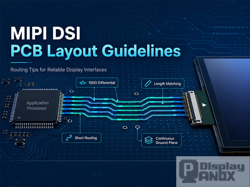
For most MIPI DSI and D-PHY display designs, the target differential impedance is 100Ω. A tolerance of ±10% is a practical rule for many display boards, unless the SoC vendor, display driver IC, or module datasheet gives a different requirement.
Impedance control matters because every discontinuity creates reflection. The reflection may come from a trace width change, connector pad, via transition, sharp neck-down area, poorly controlled FPC connector footprint, or an incorrect PCB stack-up. One small discontinuity may not destroy the link, but several small discontinuities along the same high-speed path can reduce eye diagram margin quickly.
A common mistake is to check only DC continuity or low-frequency resistance. MIPI problems are usually high-frequency problems. A trace can pass a multimeter check and still perform poorly in high-speed mode. For mature projects, impedance should be confirmed with the PCB manufacturer based on the final stack-up, copper thickness, dielectric constant, solder mask condition, and trace geometry.
Practical layout rules:
-
Use 100Ω differential impedance as the default MIPI DSI target.
-
Confirm the impedance calculation with the PCB manufacturer before fabrication.
-
Avoid sudden trace width changes.
-
Keep the pair geometry consistent through the route.
-
Pay special attention to connector pads and BGA escape areas.
-
Do not treat the FPC connector as an “ideal wire”; it is part of the signal path.
4. Length Matching: Control Both Intra-Pair and Inter-Pair Skew
MIPI differential pairs must be length matched. There are two levels of matching:
First, the positive and negative traces inside the same differential pair should be closely matched. This is called intra-pair length matching. For a strict and practical display PCB rule, keep the mismatch within:
≤12 mil, about 0.3 mm
Second, different MIPI lanes should also be controlled against each other. This includes matching between data lanes and, depending on the design requirement, between data lanes and the clock lane. A practical quick rule is:
≤36 mil, about 0.9 mm
These values are not meant to replace the SoC vendor’s official timing budget, but they are useful as a conservative layout target for compact display boards. When the data rate becomes higher, the unit interval becomes smaller, and skew tolerance becomes tighter. A length difference that is acceptable at a lower speed may become risky at a higher speed.
Length tuning should also be done with care. Long serpentine patterns can introduce additional coupling, impedance variation, and mode conversion. The best length matching is achieved by clean placement and short routing first, then small local tuning only where necessary.
Good practice:
-
Match P/N inside each pair first.
-
Then match lane-to-lane length.
-
Avoid excessive serpentine tuning.
-
Keep tuning structures away from connectors and via transitions.
-
Do not place dense serpentine sections too close to other high-speed pairs.
-
Keep the pair spacing consistent inside tuning areas.
5. Trace Length: Keep the MIPI Route Short
For compact display products, PanoxDisplay recommends keeping the MIPI differential route below:
<6 inches, about 152 mm
This is a practical design limit for many display boards using standard FR-4 material and common connector structures. Shorter is always better.
As the trace becomes longer, insertion loss increases and the high-frequency components of the signal are attenuated. The result is slower rising and falling edges, reduced eye height, reduced eye width, and less margin at the receiver. The display may still work in a lab test at room temperature, then fail after cable changes, panel replacement, temperature drift, or mass production tolerance.
If the mechanical structure forces a longer MIPI path, several options should be considered:
-
Move the display connector closer to the processor.
-
Use a better PCB stack-up and lower-loss material.
-
Reduce display resolution, refresh rate, or color depth if the product allows it.
-
Use DSC or other supported compression methods where available.
-
Add a bridge, retimer, or display controller board when the system architecture requires it.
-
Run signal integrity simulation instead of relying on generic layout rules.
For high-resolution displays, long MIPI routing should not be treated as a simple PCB drawing issue. It is a system-level design decision.
6. Keep a Continuous Ground Reference Plane
Every MIPI differential pair needs a stable return path. In most PCB designs, this means routing the MIPI lanes over a continuous ground plane.
The ground reference plane under the MIPI traces should not be split, cut, or interrupted. Avoid routing across gaps between ground islands, power plane openings, large anti-pads, or dense via arrays that block return current. If the return path is forced to detour, the loop area increases, which can increase EMI and degrade signal integrity.
A clean reference plane is especially important near:
-
SoC BGA escape areas
-
Display FPC connector pads
-
Board-to-board connectors
-
Layer transition vias
-
EMI/ESD protection areas
-
Power plane boundaries
-
Mechanical cutouts or slots
If the MIPI pair changes layers, place ground stitching vias near the signal vias to provide a short return path. The via transition should be symmetrical for the positive and negative traces. Avoid using a different number of vias on the two traces of the same pair.
Good practice:
-
Route MIPI lanes over solid ground.
-
Do not cross split planes.
-
Keep return current paths short.
-
Add ground stitching vias near layer changes.
-
Use the same via structure for P and N.
-
Avoid unnecessary layer changes.
7. Via Control: Fewer Vias, Better Symmetry
Vias are one of the most common sources of impedance discontinuity in MIPI routing. A via adds parasitic capacitance, parasitic inductance, and sometimes a stub. At high speed, the via is not just a hole; it is a discontinuity in the channel.
A practical quick rule is:
No more than 4 vias on a MIPI differential path
When vias cannot be avoided, place them in matched pairs and keep the via count equal on P and N. Add nearby ground stitching vias to improve the return path. For higher-speed designs, via stub length should also be controlled. Back drilling, blind vias, buried vias, or optimized pad stacks may be needed in advanced boards.
Recommended rules:
-
Avoid vias when possible.
-
Keep via count low.
-
Use the same number of vias on both traces in a pair.
-
Place P/N vias symmetrically.
-
Add ground stitching vias near signal vias.
-
Avoid long via stubs.
-
Do not place multiple uncontrolled vias near the display connector.
8. Spacing and Crosstalk: Use the 3W Rule
MIPI lanes should not be crowded together without spacing control. Crosstalk can come from other MIPI lanes, clocks, power switching nodes, memory buses, DC/DC converters, or unrelated high-speed interfaces.
A practical rule is the 3W rule, where W is the trace width:
-
MIPI differential pair to another differential pair: ≥3W
-
MIPI pair to other signal traces: ≥3W
-
Minimum differential pair spacing target: 15 mil where layout space allows
If a ground guard is used on the surface layer, it should be connected with stitching vias. For surface ground shielding, a practical via pitch rule is:
-
Ground stitching via pitch: ≤200 mil
-
Clock-related surface guard via pitch: ≤300 mil
Ground guarding is useful only when it is implemented correctly. A floating copper guard or a ground guard without enough stitching can create new resonance and coupling problems. In tight areas, it is often better to maintain clean pair geometry and a solid reference plane than to force decorative copper between traces.
9. Power Decoupling for MIPI PHY and Display Driver IC
MIPI signal quality is also affected by power quality. The PHY power pins, display driver IC power rails, and connector-side power supply should be decoupled properly.
Common rails around display interfaces may include AVDD, DVDD, IOVDD, DOVDD, VCI, VDDIO, or panel-specific power domains. The exact naming depends on the display IC and host platform.
A practical decoupling approach:
-
Place high-frequency MLCC capacitors close to the related power pins.
-
Use short and wide traces from capacitor to pin.
-
Connect capacitors to ground with short vias.
-
Use 100 nF capacitors for high-frequency decoupling where recommended.
-
Add 1 µF to 10 µF bulk capacitance for lower-frequency ripple.
-
Follow the panel IC and SoC vendor reference design first.
-
Separate noisy switching power areas from MIPI signal routing.
A decoupling capacitor placed far away from the power pin has much less effect at high frequency. Long capacitor traces add parasitic inductance, reducing the ability of the capacitor to suppress fast transient noise. In compact display boards, placement is often more important than simply adding more capacitors.
For sensitive display systems, a dedicated LDO or well-filtered power rail can help isolate the MIPI PHY or display driver IC from noisy system power.
10. MIPI DSI PCB Layout Quick Reference Table
The following table summarizes practical routing rules for compact MIPI DSI display PCB design.
| Parameter | Recommended Requirement |
|---|---|
| Differential impedance | 100Ω ±10% |
| Intra-pair length matching | ≤12 mil, about 0.3 mm |
| Inter-pair length matching | ≤36 mil, about 0.9 mm |
| Maximum trace length | <6 inches, about 152 mm |
| Maximum via count | ≤4 vias, placed in matched pairs with ground stitching vias |
| Ground stitching via pitch near pair vias | ≤30 mil, about 0.76 mm |
| Spacing between differential pairs | ≥3W, minimum 15 mil where possible |
| Spacing to other signals | ≥3W |
| Surface guard ground via pitch | ≤200 mil; clock-related guard via pitch ≤300 mil |
| Reference plane | Continuous solid ground plane |
These numbers are useful for early layout control and design review. For high-resolution displays, high refresh rate products, long FPC paths, or unusual stack-ups, the final design should still follow the host processor datasheet, display IC requirements, and signal integrity simulation results.
11. Common MIPI PCB Layout Mistakes
Several layout mistakes appear repeatedly in failed or unstable MIPI display projects.
11.1 Routing Across a Split Plane
A MIPI pair routed across a split ground or power plane loses its clean return path. This can increase EMI and cause reflection or mode conversion. The trace may look short and neat on the top layer, but electrically the return current has to find a longer path.
11.2 Unequal Via Structures
If the positive trace has one via and the negative trace has two vias, the pair is no longer balanced. Even if the length is later adjusted, the via discontinuity remains different on both sides.
11.3 Over-Tuned Serpentine Traces
Length matching is important, but excessive serpentine routing can create coupling and impedance problems. Clean placement is better than aggressive tuning.
11.4 Poor Connector Footprint Control
MIPI often passes through fine-pitch FPC connectors. Large pads, sudden neck-down traces, and poorly controlled anti-pad areas can create impedance discontinuity. Connector breakout should be reviewed carefully.
11.5 Decoupling Capacitors Placed Too Far Away
Adding capacitors is not enough. The loop from power pin to capacitor to ground must be short. A capacitor placed far from the IC may look correct in the schematic but perform poorly on the actual board.
11.6 Treating All MIPI Panels the Same
Different display modules may use different lane counts, clock rates, initialization sequences, voltage rails, connector pinouts, and timing requirements. A layout that works for one 720p panel may not be safe for a higher-resolution OLED or Micro OLED module.
12. Practical Design Flow for MIPI Display PCB
A reliable MIPI display board should be planned before routing begins.
First, confirm the display interface: lane count, DSI mode, color depth, refresh rate, power rails, connector pinout, reset signal, backlight or OLED power requirement, and initialization sequence.
Second, estimate the required bandwidth. The MIPI lane count and data rate must support the target resolution and frame rate with enough margin.
Third, define the PCB stack-up with the board manufacturer. The trace width and spacing for 100Ω differential impedance should be calculated before layout starts.
Fourth, place the SoC, display connector, ESD devices, and power components with routing in mind. The MIPI path should be short, direct, and free from unnecessary layer changes.
Fifth, route the MIPI pairs with controlled impedance, length matching, solid ground reference, and proper spacing.
Finally, review the layout using a checklist. For critical projects, use TDR, S-parameter extraction, or eye diagram simulation to verify channel quality.
13. How PanoxDisplay Supports MIPI Display Integration
PanoxDisplay supplies LCD, OLED, AMOLED, Micro OLED, and custom display modules for embedded and industrial applications. Many of these display products use MIPI DSI because it supports compact connectors, high bandwidth, low pin count, and modern high-resolution display requirements.
For customers developing MIPI-based display systems, PanoxDisplay can support:
-
MIPI display module selection
-
Resolution, brightness, size, and interface matching
-
FPC and connector information
-
Display initialization reference
-
Touch panel integration
-
Controller board options
-
Custom display module development
-
PCB integration discussion for display-side design
A stable MIPI display design depends on both the module and the board. When the panel specification, host platform, PCB layout, and power design are considered together, the final product is much more likely to pass bring-up smoothly and remain stable in mass production.
14. Conclusion
MIPI DSI is a powerful interface for modern display systems, but it requires careful PCB layout. The most important rules are easy to remember: use controlled 100Ω differential impedance, keep the route short, match pair lengths, maintain a continuous ground reference, control vias, keep enough spacing, and place decoupling capacitors close to the relevant pins.
For many compact display boards, the key numbers are:
100Ω impedance, 12 mil intra-pair matching, 36 mil inter-pair matching, less than 6 inches trace length, 3W spacing, and matched vias with nearby ground stitching.
These rules will not replace the official SoC and display IC requirements, but they provide a strong starting point for reliable MIPI DSI PCB design. For high-resolution LCD, OLED, AMOLED, and Micro OLED display projects, early layout planning can prevent many of the random and painful problems that appear during display bring-up.
Learn more: How to Bring Up a MIPI DSI Display: A Practical Guide for Embedded Display Integration