







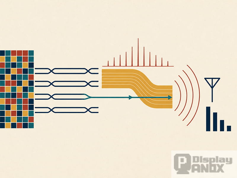
A still image looks electrically quiet. Inside a phone, however, displaying it may require a high-speed link to stream pixel data continuously. Under the wrong system conditions, MIPI DSI RF interference can occur when emissions from the DSI/D-PHY link overlap a receive band, cause RF desense and make weak cellular signals harder to detect.
In the handset-level case reconstructed here, receiver sensitivity deteriorated when the display turned on. The spectrum analyzer was reported to show narrow, evenly spaced spurs rather than a broad rise in noise, with adjacent comb teeth separated by approximately 19.23 MHz.
This is not evidence that MIPI DSI is inherently noisy. It shows how a periodic high-speed signal, an imperfect physical path and a sensitive radio can form an unintended coupling chain. The MIPI DSI specification family is designed for high bandwidth, low power and low electromagnetic interference, yet the final EMC result still depends on the processor, panel, lane configuration, connector, FPC, PCB return path, enclosure and antenna layout working as one system.
The 19.23 MHz spacing does not identify the root cause by itself. It is a reported clue that may connect the spectrum to the timing structure of the display interface. The rest of the diagnosis comes from understanding how pixels become bits, how repetitive bits become spectral lines, and how differential energy can turn into common-mode current that reaches the antenna.
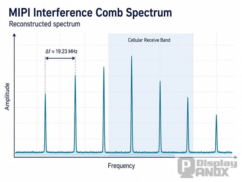
Reconstructed comb spectrum showing approximately 19.23 MHz spacing between adjacent interference peaks.
From a Static Image to a High-Speed MIPI Bitstream
In a typical mobile display path, an application processor or display controller sends pixel data to the panel through MIPI Display Serial Interface, or MIPI DSI. DSI defines the display protocol. MIPI D-PHY provides the electrical transport, commonly using a forwarded clock lane and one or more differential data lanes. The MIPI Alliance describes D-PHY as a clock-forwarded synchronous link with scalable data lanes, while AMD’s DSI-2 receiver documentation illustrates practical support for one to four lanes and several pixel formats.
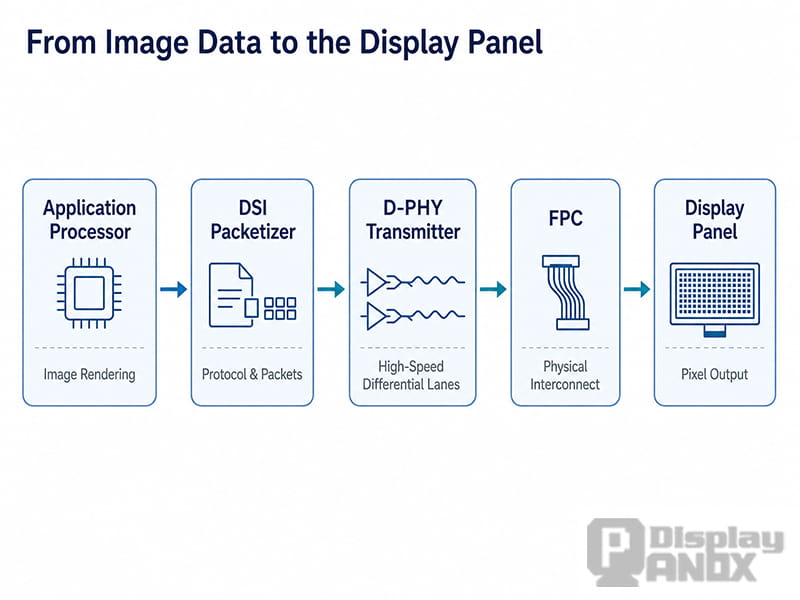
Consider a simplified four-lane configuration in which each data lane runs at 461.52 Mb/s and the display uses RGB888, or 24 bits per pixel. Ignoring blanking and protocol overhead for the moment, the aggregate raw lane rate is:
4 × 461.52 Mb/s = 1,846.08 Mb/s
Dividing that rate by 24 bits per pixel gives an ideal active-pixel throughput of 76.92 million pixels per second. Under the simplified assumptions used in this case, that payload-derived value is presented as an approximate 76.92 MHz pixel clock in a one-pixel-per-clock pipeline. The real panel clock cannot be established from this division alone because blanking, packet overhead, video mode and link margin also matter. In a traditional double-data-rate, clock-forwarded D-PHY implementation, a 461.52 Mb/s lane rate corresponds to a forwarded clock near 230.76 MHz.
These rates are not the only timing structures in the link. Repeating pixel content, byte packing and lane distribution can introduce additional periods, while packet, line, frame and high-speed/low-power timing impose rhythms of their own. A spectrum analyzer does not see a picture; it sees the electrical result of those periods and their edges.
An eye diagram provides another view of the same link. Thousands of 0-to-1 and 1-to-0 transitions are overlaid in a common time window, leaving an eye-shaped opening in the center. A wider and taller opening generally means more timing and voltage margin. A closing eye points to greater jitter, noise, attenuation or amplitude uncertainty.
A public NXP and Tektronix D-PHY receiver-validation case includes an eye diagram at a 2.5 Gb/s test rate. That rate belongs to the NXP calibration example, not to the 461.52 Mb/s case discussed here; the value of the example is the measurement method, not a direct numerical comparison.
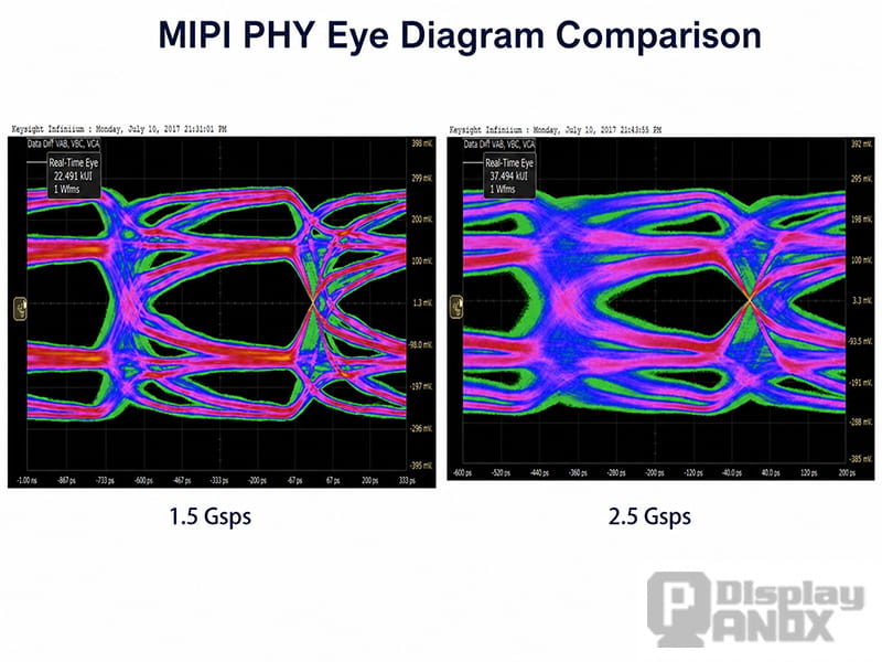
An open eye indicates adequate signal-integrity margin, but it does not rule out common-mode radiation or receiver desense.
What RGB888 Means for Display Bandwidth
RGB888 assigns eight bits to red, eight to green and eight to blue. Each color component can therefore represent 256 levels, from 0 to 255. One pixel occupies 24 bits, or three bytes, and the theoretical color space contains 16,777,216 combinations.
Other common formats make a different trade-off between color depth and bandwidth. RGB565 uses five red bits, six green bits and five blue bits for a total of 16 bits per pixel. Packed RGB666 transmits 18 bits per pixel. Loosely packed RGB666 retains 18 bits of color information but places each pixel in three bytes, so it consumes 24 transmitted bits per pixel. RGB888 transmits 24 bits per pixel and is common in mobile and embedded displays. A 30-bit RGB format, with 10 bits per component, provides finer gradation when the controller, DSI implementation and panel support it.
AMD’s MIPI DSI transmitter example explicitly identifies RGB888 as three bytes, or 24 bits, per pixel.
For a first-order estimate, active-image throughput follows a simple relationship:
aggregate active-pixel payload rate ≈ pixel rate × transmitted bits per pixel
Real links also carry blanking intervals, packet headers, error checking and other overhead, so a production calculation must use the complete panel timing and DSI mode. The simple equation is still useful because it shows why higher color depth, resolution or refresh rate usually demands more link bandwidth.
Lane count changes how that bandwidth is transported. With one active lane, every bit passes through the same serial path. With four lanes, the controller distributes traffic across four paths so that the same total throughput can be achieved at a lower required rate per lane. At 461.52 Mb/s, one unit interval—the time occupied by one bit on one lane—is about 2.17 ns.
A lane must not be treated as a permanent red, green or blue channel. DSI first creates protocol packets, after which the lane-management layer distributes the protocol byte stream across the active lanes and each lane serializes its assigned bytes.
The apparent symmetry of three color bytes and three lanes does not prove a one-color-per-lane mapping. Changing from four lanes to three can be an excellent diagnostic experiment, but it changes more than a single variable: lane rate, byte distribution, repeating periods and the spectrum may all move together.
Why Different Bit Patterns Produce Different EMI Spectra
High data rate alone does not determine the shape of a spectrum. The order of the zeros and ones matters because transitions occur at different times and with different repetition periods.
A long run such as 00000000 or 11111111 contains few transitions within the observation window. In an idealized model, its high-frequency content is relatively low.
The alternating pattern 01010101 changes state at every bit boundary and repeats every two bits, concentrating energy at a well-defined fundamental and its harmonics. The pattern 00110011 also repeats, but its four-bit period produces a lower fundamental repetition frequency.
A more random sequence still contains many transitions, yet their timing is less dominated by one short period, so the energy is usually spread across more frequencies instead of piling up in a few tall lines.
More transitions do not automatically mean more interference at every frequency. A strongly periodic pattern can concentrate energy into a small number of narrow peaks, while a less repetitive sequence often distributes its switching energy over a wider band and lowers the tallest peaks. Transition density can also change the total switching energy, so the effect is not purely a redistribution problem.
Display content therefore can affect the noise generated by MIPI DSI traffic over D-PHY. Black, white, stripes, checkerboards and random images produce different pixel sequences, which can change spur amplitude in specific RF bands.
A black or white screen does not make a continuously streamed video-mode link electrically silent. DSI packet headers, error-checking fields, line and frame timing, blanking traffic, clock activity and transitions between high-speed and low-power states may remain even when the visible image is motionless.
A command-mode panel with internal memory, adaptive refresh or panel self-refresh may instead allow the link to idle between updates, so the operating mode must be included in the diagnosis.
The most useful content test asks two separate questions: does the spacing between the comb teeth move, and do their amplitudes change? If image content changes the height of the teeth while their positions remain nearly fixed, the result supports a model in which the interface timing sets the comb spacing while the bit pattern and edge timing shape the amplitudes.
Comb Spacing and Spur Height Are Different Clues
Any structure that repeats every T seconds can produce spectral components spaced by approximately 1/T. The repetition period therefore helps determine where the comb teeth appear.
Their height depends on what happens inside each period. Duty cycle, edge speed, transition density and the phase relationship between edges can make contributions add or cancel at a particular frequency. Several transitions arriving with the same phase can reinforce one spur; different timing can reduce it.
This is why a tall spur cannot be explained by the clock frequency alone. A complete explanation must identify which edges reinforce one another at that frequency.
This distinction is central to MIPI DSI EMI troubleshooting. Timing tends to establish the available spectral locations; payload and transition structure redistribute energy among them.
Why Differential MIPI Signals Can Still Reach the Antenna
An ideal differential pair carries equal and opposite currents. The fields produced by the two conductors largely cancel, which is one reason MIPI D-PHY can carry high data rates with relatively low EMI. Real products are never perfectly symmetrical.
Skew between the positive and negative traces, unequal losses, impedance discontinuities, connector geometry, via transitions, FPC construction and an interrupted or poorly defined return path can unbalance the pair. Some differential-mode energy is then converted into common-mode energy.
Common-mode current moves in the same direction on both conductors relative to the reference structure and can use an FPC, shield, chassis or other metal as a more effective radiator. This is the physical basis of MIPI D-PHY common-mode noise.
STMicroelectronics demonstrates how differential-pair skew creates common-mode radiation, while Murata documents how MIPI D-PHY noise can propagate along an FPC and enter an antenna.
The resulting failure chain has three parts: a source, a coupling path and a victim. D-PHY transitions in the display subsystem provide periodic energy; the connector, FPC, PCB and enclosure provide a path; the cellular antenna and receiver become the victim.
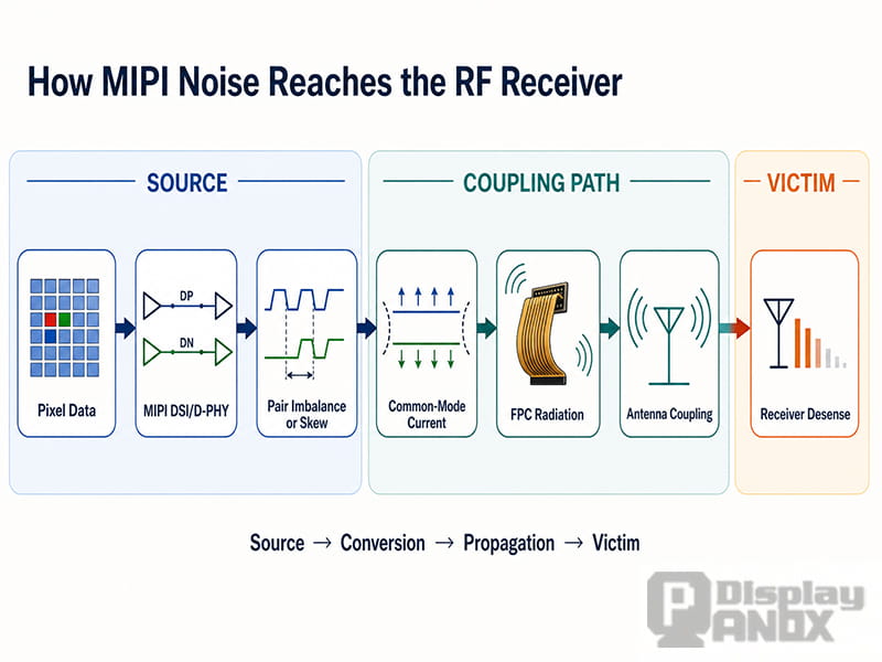
Receiver desense occurs when coupled interference raises the effective in-band noise floor or otherwise reduces sensitivity to the wanted signal. In a handset, this failure is commonly described as smartphone RF desense.
This mechanism has been measured in real hardware. A 2017 paper in IEEE Transactions on Electromagnetic Compatibility, “Physics-Based Dipole Moment Source Reconstruction for RFI on a Practical Cellphone”, reconstructed an equivalent source at the edge of the display flexible printed circuit board and validated the coupling from the LCD assembly to the phone’s cellular antenna through near-field measurements.
A separate public wireless and IoT case from EMC consultant Kenneth Wyatt found a strong video-related signal leaking from the edge of a PCB into LTE Band 5. After frequency-appropriate absorber material was applied at three places—a memory device, a hot flex cable and a power-management IC—the unwanted signal fell by at least 15 dB and receiver sensitivity improved.
The AltiumLive case study does not isolate the contribution of each patch or establish MIPI DSI as the source. Its value is the practical demonstration of localization and band-matched mitigation, not evidence that absorber material is a universal cure.
What the 19.23 MHz Comb Spacing Really Tells Us
The illustrative case contains a striking numerical relationship:
| Parameter | Value |
|---|---|
| Per-lane data rate | 461.52 Mb/s |
| Forwarded D-PHY clock | approximately 230.76 MHz |
| Ideal active-pixel throughput, ignoring overhead | 76.92 Mpixel/s |
| Reported comb spacing | approximately 19.23 MHz |
Two divisions arrive at the same result:
461.52 ÷ 24 = 19.23
76.92 ÷ 4 = 19.23
Numerically, dividing the per-lane bit rate by the 24-bit RGB888 word length and dividing the ideal active-pixel throughput by the four active lanes both produce 19.23 million per second.
These ratios are rearrangements of the same simplified payload equation rather than independent evidence. They make a display-related period worth testing, but neither defines a universal DSI timing period or establishes a physical 24-UI or four-pixel repetition on any lane.
Pixel data is packetized and byte-striped across lanes, and dividing pixel rate by lane count has no independent protocol meaning. The agreement is a clue, not proof of a specific mechanism.
The relationships do not prove that one 24-bit RGB word is the unique cause. Multi-lane distribution, packet framing, line and frame blanking, controller architecture and panel-specific implementation can all create or modify the repeating structure. Several internal periods may also share the same fundamental divisor.
The disciplined interpretation separates reported inputs from verified mechanisms. The lane rate, pixel format and comb spacing are the stated parameters of the illustrative case. A particular byte-to-lane mapping, a physical 19.23 MHz repetition or a claim that RGB888 alone creates the comb remains a hypothesis until actual lane traffic, configuration documentation or a controlled rate-change experiment confirms it.
The 19.23 MHz spectrum discussed in this case is a structural reconstruction based on the test parameters rather than a raw spectrum-analyzer capture. Product-level conclusions must always be checked against the real protocol configuration, measured waveform and receiver response.
A Test Plan That Can Change the Conclusion
The fastest route to a credible root cause is a set of controlled changes that produce different predictions for competing explanations.
Change the MIPI Lane Rate Slightly
A small, supported adjustment to the lane rate is the most direct first experiment. If the comb spacing moves in proportion to the new rate, the result strongly supports a MIPI timing origin. It still does not identify whether the decisive period comes from pixel packing, lane distribution, packet timing or blanking structure.
Change the Displayed Pattern Without Changing Link Timing
With resolution, refresh rate, lane rate, panel timing, compression state and operating mode held constant, the display can cycle through black, white, stripes, a checkerboard and a pseudo-random image.
Stable comb positions with changing amplitudes support the distinction between timing and payload: timing sets the positions, while data patterns influence the energy at those positions.
Change Lane Count or Refresh Rate
Changing lane count or refresh rate is useful for discovering correlation. It also changes several linked variables, so it should not stand alone as final proof. A four-to-three-lane test may alter per-lane rate, byte scheduling and packet periodicity at the same time.
Close the Source–Path–Victim Evidence Chain
A near-field probe can scan the SoC, display connector, FPC and panel edge for the same spectral signature. An RF current probe can then look for common-mode current on the flex or other conductors.
Finally, calibrated receiver sensitivity should be measured while the suspected source and path are changed, together with the relevant BER, BLER, PER, throughput or TIS result. RSSI can provide supporting information, but it is not sufficient proof because interference may raise RSSI while reception becomes worse.
Finding the same comb at an FPC edge identifies a possible source or radiator. It does not prove desense if receiver performance remains unchanged. The evidence chain closes only when the spectral signature, spatial hotspot, coupling path and receiver degradation move together.
How to Reduce MIPI DSI RF Interference
Effective countermeasures act on one of three things: the spectral position, the concentration of energy or the coupling path. A filter added without a mechanism may hide one symptom while degrading the display eye or moving the problem elsewhere.
Move Harmonics Away from the Active RF Channel
Changing the MIPI lane rate can move the comb and its harmonics away from a cellular, GNSS or Wi-Fi receive band.
A 2024 Technical Disclosure Commons publication describes dynamically selecting MIPI frequency and spread-spectrum clocking state according to the communication channel in use.
A related 2025 Sony study used RSSI feedback to adapt a camera MIPI D-PHY data rate and reported about 9.1 dB of interference mitigation on its test platform. Although the Sony case concerns an imaging link rather than a display link, it supports the broader principle that controlled MIPI rate adjustment can move radiated noise out of a vulnerable channel.
Spread Narrow Peaks
Spread-spectrum clocking and data scrambling can reduce the height of narrow spectral peaks by distributing energy over a wider frequency range.
A MIPI Alliance white paper notes that DSI-2 supports data scrambling to lower EMI and reduce shielding needs. Scrambling is not a universal feature of every legacy DSI link or every current controller, so both ends of the implementation must support it.
These techniques reduce peak spectral density rather than eliminating energy, which means adjacent channels and all operating modes still require validation.
Reduce Differential-to-Common-Mode Conversion
The most fundamental layout work preserves symmetry. The two traces in each pair need closely matched geometry and delay, controlled differential impedance, clean reference planes and well-designed transitions through connectors and FPCs.
Return paths should remain continuous across layer changes and mechanical boundaries. The connector pinout, ground placement, FPC stack-up and bend geometry deserve the same attention as the PCB traces because a balanced pair can become unbalanced at a single poor transition. Panox’s MIPI DSI PCB layout guidelines provide additional display-side routing context.
Power integrity also matters. Noise on PHY, display-driver or panel rails can modulate edge timing and common-mode voltage even when the nominal differential routing looks correct. Tektronix D-PHY test coverage explicitly includes differential mismatch and dynamic common-mode measurements, which reflects the importance of both signal-integrity and common-mode behavior.
Contain the Confirmed Path
A common-mode choke, local shield or ferrite-loaded absorber can be effective when it is selected for the target band and placed on a confirmed path.
Each addition must be checked for insertion loss, mode conversion, eye opening and protocol reliability. Absorber material that performs well at microwave frequencies may do very little in a lower cellular band; a common-mode component with excessive differential loading can damage the MIPI eye.
Consider Interface Architecture Early
EMC is increasingly part of the interface architecture rather than a patch added at the end.
The MIPI DSI-2 v2.1 update added support for the optional embedded-clock feature in D-PHY v3.5, which MIPI highlights for applications with stringent EMI, power and pin-count requirements.
Such options only help when the host, panel and complete implementation support them, but they show the direction of modern display-link design.
A Panox Display Integration Perspective
From a Panox Display integration perspective, a display module is not an isolated optical component. Pixel format, refresh rate, lane count, lane rate, clock mode, connector location, FPC construction and controller-board design all affect the electrical behavior of the finished product.
Panox’s existing MIPI DSI display bring-up guide covers the configuration work that should be settled before RF coupling is investigated.
Panel selection should therefore be reviewed together with the processor’s DSI capabilities, required throughput, available frequency plan and mechanical route from the host to the display. Early flexibility in lane rate, refresh mode, FPC geometry and connector grounding is far less expensive than an absorber or shield added after the enclosure and antenna positions are frozen.
Panox Display supports mobile display selection for MIPI DSI projects, together with panel-specification review, host matching, timing and connector information, FPC requirements and controller-board evaluation. The goal is a display that starts reliably, meets its bandwidth and timing requirements, and coexists with the product’s wireless subsystem.
The Complete Cause-and-Effect Chain
A quiet picture can be carried by a very active electrical interface. When pixel data creates a repeating bitstream, that periodicity can appear as a comb of MIPI harmonics. Bit patterns and edge phase determine how strongly energy collects at individual teeth.
Imperfect balance in the D-PHY pair, connector or FPC can convert part of that energy into common-mode current, and the surrounding structure can couple it into the antenna. The receiver then experiences in-band interference and reduced usable sensitivity.
The complete physical chain is:
pixels → DSI packets and bitstream → periodic edges → spectral comb → common-mode leakage → antenna coupling → receiver desense
The important questions are no longer limited to the frequency of a single spur. A useful diagnosis explains why the spur appears at that frequency, why it reaches that amplitude and how it enters the receiver.
With those three answers, MIPI DSI RF interference becomes a testable engineering problem rather than an unexplained conflict between the screen and the antenna.
Learn more: MIPI DSI PCB Layout Guidelines for Reliable Display Interfaces