







An 8-bit grayscale value of 128 describes a shade. To display that shade, the panel needs a row-select pulse, a column voltage that settles in time, and a pixel circuit that holds the programmed value until the next refresh. A display driver IC (DDIC) converts image data from the host processor into the electrical signals that make this sequence possible.
The DDIC and the panel’s thin-film transistors, or TFTs, work at different points in that sequence. A TFT is fabricated on the panel backplane and acts as a switch, a drive transistor, or part of a larger pixel circuit. A DDIC is typically a silicon chip that controls groups of pixels by supplying data and timing signals. In a chip-on-glass (COG) assembly, the die is bonded directly to the panel glass. In a chip-on-film (COF) assembly, it sits on a flexible carrier that connects to the panel. COF bonding and LCD module assembly
This division of work explains much of the difference between TFT LCD and AMOLED. An LCD pixel uses a stored voltage to regulate how much backlight passes through the liquid crystal. An AMOLED pixel uses a drive transistor to regulate how much current flows through its own light-emitting element. Both depend on the DDIC, but they place different demands on its timing, analog outputs, and compensation functions.
From the Application Processor to the Pixel
The application processor (AP) or system-on-chip (SoC) sends image data and control commands to the display module. MIPI DSI is widely used in smartphones and other compact products. Embedded modules may use SPI or parallel RGB, depending on bandwidth, pin count, and the panel’s interface. Some modules receive image data and configuration commands over separate paths. Display interface guide for SPI, RGB, MIPI DSI, and LVDS
Inside an integrated DDIC, the interface receiver decodes the incoming data and routes configuration commands to registers. Those registers may set the pixel format, active display region, or supported operating mode. The timing controller then coordinates line and frame timing, including blanking intervals where required. The gamma reference circuit and digital-to-analog converter (DAC) map digital grayscale codes to the analog levels used to program the pixels.
The gate driver and source driver meet at the pixel. The gate driver selects a row by switching its TFTs on. The source driver applies the data level for each column while that row is selected. When the row closes, its pixels retain their programmed state and the driver moves on to the next row. Some modules integrate timing, source, and gate functions in one chip. Others use a separate timing controller or implement the gate scan on the panel backplane.
LCD and AMOLED Pixel Driving
The 1T1C TFT LCD Pixel
A TFT LCD uses a backlight, polarizers, a liquid crystal layer, and color filters. The pixel voltage changes the orientation of the liquid crystal molecules, which changes the amount of backlight that passes through the optical stack. Each red, green, and blue subpixel contributes to the final color.
A simplified 1T1C subpixel has one switching TFT and one storage capacitor. When a gate pulse turns the TFT on, the source line charges the pixel electrode to the programmed voltage. When the TFT turns off, the storage capacitor and the liquid crystal cell’s own capacitance help hold that voltage until the next refresh. The voltage across the liquid crystal is the difference between the pixel electrode and the common electrode, VCOM. LCD drive schemes normally alternate that voltage’s polarity to limit sustained DC bias across the cell.
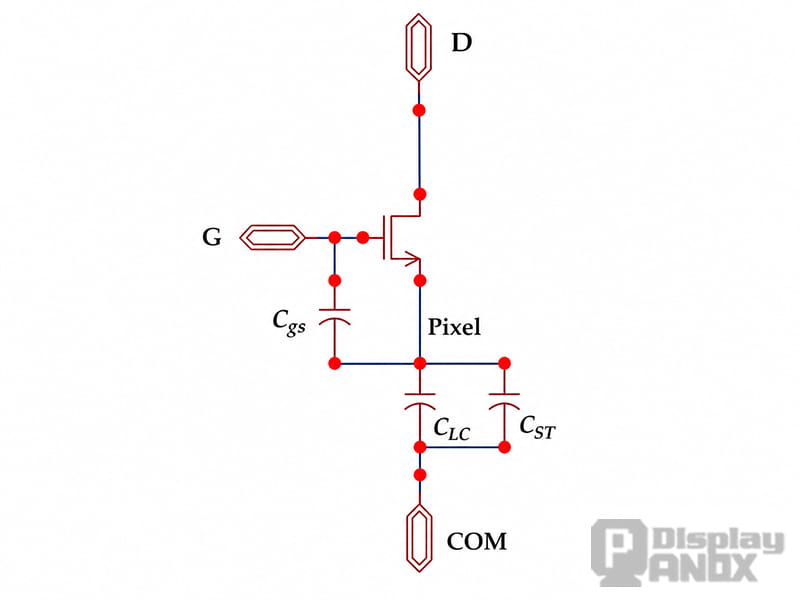
In a 1T1C TFT LCD pixel, the switching TFT writes the column voltage to the pixel node. The storage capacitor helps hold that voltage after the TFT turns off.
The switching TFT still matters. Its on-resistance affects how quickly the pixel charges, and its off-state leakage affects how well the pixel holds its voltage. A weak gate pulse, a source output that settles too slowly, or an incorrect VCOM setting can all affect the image, even though the liquid crystal responds primarily to voltage.
The 2T1C AMOLED Pixel
An AMOLED panel uses an active-matrix backplane to control light-emitting subpixels. The organic emitters generate light directly, so the optical stack has no backlight. The basic 2T1C circuit illustrates how the display programs the emitters. A switching TFT writes the data level to a storage node. A second TFT uses the stored gate bias to set the current through the OLED during emission.
In a common voltage-programmed AMOLED design, the DDIC outputs a data voltage, and the pixel’s drive TFT regulates the OLED emission current. The distinction matters when comparing LCD and AMOLED display drivers. Both can send a voltage down a column line, but the LCD uses the stored voltage to control light transmission, while the AMOLED pixel converts its programmed bias into light-producing current.
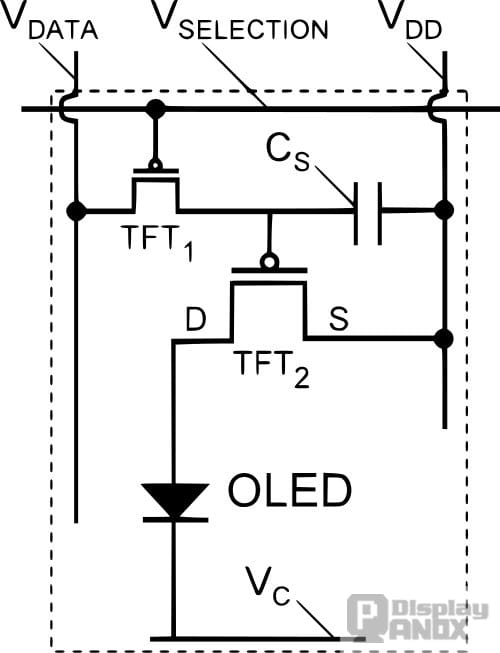
In this 2T1C AMOLED pixel, TFT₁ writes the data voltage and the storage capacitor holds the programmed gate bias. TFT₂ controls the current through the OLED.
Why AMOLED Pixels Need Compensation
Two drive TFTs can receive the same data voltage and produce different currents. Threshold voltage, or VTH, varies with the fabrication process and can shift under electrical stress. Carrier mobility, supply voltage drop across the panel, and aging of the OLED material also affect luminance. A spatial variation that shows up as a patch, band, or uneven low-gray field is often called mura.
A simplified saturation model illustrates how sensitive the current can be. With the same transistor geometry and mobility, the current varies approximately with the square of the gate overdrive, (VGS − VTH)². At a gate-to-source voltage of 2.6 V, a threshold shift from 0.8 V to 1.2 V reduces the overdrive from 1.8 V to 1.4 V. A pixel that would carry 10 µA in the first case would carry about 6 µA in the second. The calculation illustrates the effect of threshold variation in a simplified circuit.
Production panels can address this variation in several ways. Additional transistors and capacitors in the pixel circuit can sample and compensate for the drive TFT’s threshold voltage during programming. Some architectures sense pixel characteristics externally and adjust the data supplied to the panel. Optical Demura works from measured luminance or color at selected gray levels. The resulting spatial correction data is applied in the DDIC or elsewhere in the display pipeline, depending on the design. Electrical pixel compensation and optical Demura can be used together. OLED display driver IC architecture and pixel compensation
LCD Driver ICs, TDDI, and AMOLED DDICs
A conventional LCD driver IC, sometimes called an LDDI, handles the display while a separate controller handles touch, if the module has it. This is a familiar arrangement for instrumentation, industrial displays, and automotive panels. The display and touch electronics can be selected independently, with the trade-off of additional components and interconnects.
Touch and display driver integration (TDDI) combines the two functions in one IC. In an in-cell LCD implementation, the chip controls the display and reads the capacitive touch electrodes within the display stack. Combining those functions can reduce component count and simplify routing. A thinner module is possible when the sensor is integrated into the panel structure. In-cell describes where the touch sensor is located. TDDI describes how its electronics are integrated.
An AMOLED display driver IC is designed around a self-emissive panel’s programming and emission sequence. Grayscale accuracy, low-brightness uniformity, and compensation are central to its design. Some AMOLED modules use a separate touch controller, while others combine touch and display in an AMOLED TDDI. Novatek’s 22 nm AMOLED TDDI is one example of the latter.
Why Touch Timing Matters in TDDI
A source line can change voltage quickly as the display writes a row. That transition can couple into nearby touch electrodes and disturb the small capacitance changes that the touch circuit is trying to measure. Integrating both functions gives the IC a way to coordinate their timing, but the shared electrical environment still has to be managed.
Some in-cell LCDs divide each frame into display-writing periods and quieter touch-sensing windows. During a sensing window, the touch analog front end (AFE) measures the electrode signals while display switching is reduced or paused. The exact schedule varies by panel. At higher refresh rates, the timing budget has to accommodate both pixel settling and touch scanning. In-cell, on-cell, and OGS touch screen structures
Inside the DDIC Architecture
A display driver IC block diagram brings together three kinds of circuitry. Digital logic organizes the data and schedules the scan. Analog circuits convert grayscale codes into precise electrical levels. High-voltage devices translate control signals and drive the panel lines. The scan path and the column data path run in parallel and have to meet at the right moment.
Digital Logic and Timing Control
The interface receiver, command decoder, registers, and timing controller form the digital section. Some chips also include graphics RAM or a frame buffer, along with circuits for data formatting and grayscale mapping. A command-mode design may refresh the panel from local memory. A video-mode design may instead process a continuous stream with a smaller buffer. An oscillator or phase-locked loop (PLL) can provide internal clocks. Dense, low-voltage core transistors suit these functions.
Gamma, DAC, and Source Output Buffers
The gamma reference establishes the electrical levels used to reproduce the panel’s grayscale response. The DAC selects or generates an analog level for the incoming code. The source output buffer then charges the column line and settles to that level within the available row time. DAC resolution controls how finely the output can be stepped. Reference stability, transistor matching, noise, and buffer settling determine how consistently those steps appear across channels.
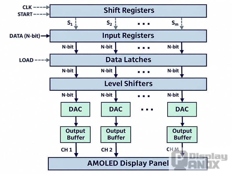
A simplified AMOLED column driver. It latches one row of digital pixel values, converts them to analog voltages, and drives the corresponding panel columns in parallel.
The timing constraint becomes clear at higher refresh rates. For a simplified 1,080-row scan, a 60 Hz frame allows about 15.4 µs per row before blanking and other overhead. At 120 Hz, the corresponding budget falls to about 7.7 µs. A source output that settles too late can leave a pixel with a different voltage from the intended one. Small errors can be especially visible in dark gradients. OLED gamma calibration and reference voltages
Level Shifters and High-Voltage Outputs
A level shifter translates a control signal from the low-voltage logic domain into a signal referenced to a higher-voltage domain. The output stage then drives the panel load. The required rails come from power-management circuitry, which may include charge pumps, boost converters, and bias regulators inside the module or in a separate IC.
In a TFT LCD, the gate driver may use a positive VGH rail to turn on the switching TFTs and a lower, sometimes negative, VGL rail to turn them off. The source driver and VCOM circuit have their own supply and reference requirements. An AMOLED panel may use different rails for source outputs, scan and emission control, and OLED current supply. ESD protection and I/O circuits protect the interfaces. TDDI adds a touch AFE and controller, while some AMOLED DDICs add memory and processing for gamma, mura, or aging compensation. How VGH and VGL are generated in TFT LCD modules
Why Display Driver ICs Use Different Process Nodes
Choosing a DDIC process node involves four practical questions. How much digital logic and memory must fit on the die? How well can the analog devices match and settle? Which voltage ratings and isolation options are available? And what will the design cost at the required volume and yield?
Smaller nodes can fit more digital logic and SRAM into a given area, which helps when a driver needs more buffering or compensation data. Analog accuracy depends on device matching, noise, reference quality, and voltage headroom. High-voltage output devices also need physical space for isolation and voltage handling. A mature node can therefore be a good fit for a driver whose area and performance are dominated by output channels.
| Process node | Example uses and design considerations |
|---|---|
| 150 nm and above | Mature high-voltage platforms for conventional LCD drivers, including large-panel, industrial, and other cost-sensitive designs. |
| 110 nm | Established display-driver platforms, with examples in LCD and automotive applications. |
| 90 nm | Mature display-driver platforms for compact displays and selected LCD designs, with more room for integrated logic. |
| 55 nm | Integrated LCD drivers and TDDI. Foundries have also offered 55 nm high-voltage options for OLED drivers. |
| 40 nm | An established AMOLED DDIC platform that can combine denser logic and memory with the analog and high-voltage devices needed for panel drive. |
| 28 nm | Higher integration for mobile OLED DDICs. TSMC reported volume production of smartphone DDICs on its 28HV platform in 2024. |
| 22 nm | More integrated mobile drivers, including commercial 22 nm display driver ICs and AMOLED TDDI examples. |
| 14 nm eHV FinFET | A newer platform example. UMC announced foundry validation and design-kit availability for its 14 nm eHV FinFET platform in 2026. |
Embedded high-voltage CMOS (eHV) allows a foundry to offer high-voltage devices alongside logic on the same process platform. A 40 nm eHV process, for example, can accommodate digital timing, storage for calibration or Demura data, and specialized analog and output devices on one die. For a driver with fewer digital functions, the savings in logic area from moving to a finer node may be small relative to mask cost, qualification effort, or the area still needed for the outputs. The available device set matters as much as the node name.
Core, Analog, and High-Voltage Devices on One Die
The devices on a DDIC serve very different electrical loads. A core transistor may switch a logic node at around 1 V, while a high-voltage output transistor has to tolerate a much larger voltage swing and charge a panel line. Analog devices sit between these demands, with matching and noise often more important than transistor density.
| Device or structure | Design priority | Typical DDIC use |
|---|---|---|
| Core MOS | Thin gate dielectric and low-voltage operation for dense logic | Registers, timing logic, command decoding, and digital processing |
| Analog MOS | Device options and layouts chosen for matching, low noise, and adequate voltage headroom | DACs, amplifiers, bias circuits, and gamma references |
| HV MOS or eHV MOS | Higher voltage tolerance through gate dielectric, drain engineering, and isolation | Level shifters, gate and source output stages, and selected interface or protection circuits |
| Polysilicon resistor | Controlled sheet resistance and matching between resistor elements | Reference ladders, bias networks, and voltage dividers |
| Metal–insulator–metal (MIM) capacitor | Predictable capacitance, good linearity, and matching | DACs, sample-and-hold circuits, filtering, and charge pumps |
Mixed-voltage platforms can use different gate-dielectric thicknesses, well implants, and isolation structures in different regions. One way to create multiple gate oxides is to use patterned removal and regrowth in selected areas. Each extra device option can add fabrication steps, mask cost, and constraints on the wafer’s thermal budget. The exact voltage ratings and oxide thicknesses depend on the foundry process and the devices selected for the chip.
Drift Regions and Isolation
At high drain voltage, the electric field can concentrate near the drain junction. A lateral high-voltage MOS transistor can use a lightly doped drift region to spread the field over a longer distance and increase breakdown voltage. That region also adds resistance in the on-state. A DDIC designer balances the required voltage margin against output resistance, switching speed, and device area.
High-voltage switching also affects neighboring circuits. A fast output transition can couple through the substrate or supply network into a gamma reference, an amplifier, or a touch AFE. Carrier injection can trigger the parasitic PNPN path that causes latch-up, creating a sustained high-current path. Guard rings, well contacts, deep wells, and, where available, trench isolation help manage these effects. Their placement helps explain why a real DDIC floorplan gives dedicated space to high-voltage outputs, analog circuits, digital logic, and the I/O and level-shifting circuitry between them.
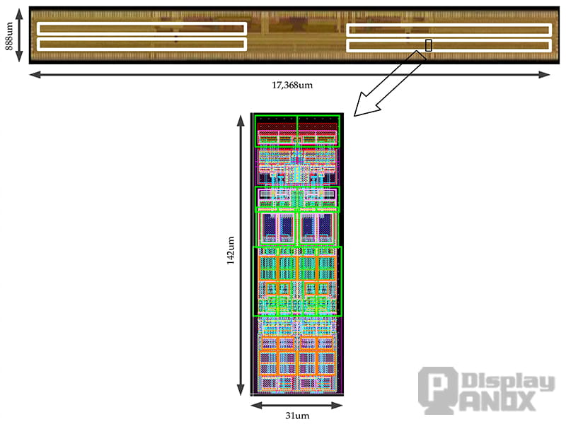
The fabricated TFT LCD column driver die measures 17.368 mm × 0.888 mm (top). The enlarged layout below shows a pair of output buffer amplifiers.
How Wafer Acceptance Testing Relates to Display Quality
Wafer acceptance testing (WAT) measures electrical characteristics on dedicated process-monitor structures, often located in the scribe lines between dies. Typical measurements include transistor threshold voltage, drive current and leakage, high-voltage breakdown, resistor sheet resistance, capacitance, and contact or via resistance. These data show how the fabrication process is behaving across wafers and lots.
The connection to image quality runs through the circuit. A change in transistor characteristics can affect amplifier offset, output settling, or timing margin. Those changes can alter the signal delivered to a panel and may show up as grayscale errors, flicker, color shift, or uneven brightness. WAT characterizes the silicon driver process. The panel backplane and optical stack have their own electrical and optical tests.
| WAT finding | Possible effect inside the DDIC | What panel testing might reveal |
|---|---|---|
| Core MOS threshold shift or lower saturation current | Reduced logic speed or timing margin | Intermittent refresh or timing-related artifacts |
| Analog MOS mismatch or transconductance variation | Amplifier offset, gain variation, or differences between DAC channels | Grayscale bands, brightness differences, or color tint |
| Higher on-resistance in high-voltage devices | Slower gate or source transitions under load | Incomplete pixel charging or row and column artifacts |
| Lower high-voltage breakdown margin or higher leakage | Reduced tolerance to electrical stress or unwanted current at an output | Intermittent line defects or reliability issues under stress |
| Resistor ratio variation or MIM capacitor mismatch | Shifted gamma references or inaccurate sampling | Gray-level errors, noise, or flicker |
| High contact, via, or metal resistance | Greater voltage drop in a bias or supply path | Regional brightness variation or mura, depending on the affected circuit |
| Excess off-state leakage | Stored analog voltages drift before the next update | Unstable dark levels or gray errors that vary with refresh rate |
Long-term mechanisms such as bias temperature instability, hot-carrier degradation, and dielectric breakdown are evaluated through related reliability monitoring and qualification. Their relevance depends on the operating voltage, temperature, and stress history of the device.
Following a Defect Back Through the Test Data
An investigation can begin with a repeatable symptom. A band that appears on a low-gray test pattern, for example, gives the engineering team a specific condition to reproduce. The first checks may include the gamma reference, source-channel output, and power rails. Wafer maps can then show whether the suspected electrical parameter is concentrated in a wafer region or manufacturing lot.
Chip probe (CP), or wafer sort, tests the actual dies. Final test (FT) checks the assembled or packaged driver where applicable. Panel testing then evaluates the complete display under defined patterns, gray levels, refresh rates, and temperatures. A convincing diagnosis links the same failure mechanism across those stages. When the results point in different directions, the investigation can move to panel bonding, power integrity, timing configuration, or the panel backplane. A visible defect such as mura can originate in any of these parts of the display system.
What the DDIC Means for Display Module Selection
Two modules with the same resolution and interface can require different initialization commands, bias rails, scan timing, or touch arrangements. The DDIC determines many of those requirements, and the panel determines how the signals are used. For a design with a tight row-time budget, source settling may deserve particular attention. For an AMOLED module used at low brightness, grayscale uniformity and the panel’s calibration matter more than the process node alone.
At Panox Display, we review the driver and panel together when matching a module to a host platform. The starting points are the interface and initialization sequence, followed by power and reset timing, refresh rate, touch configuration, and the image performance needed in the application. This is especially useful when comparing modules that look similar on a specification sheet. TFT LCD display modules · AMOLED display modules