







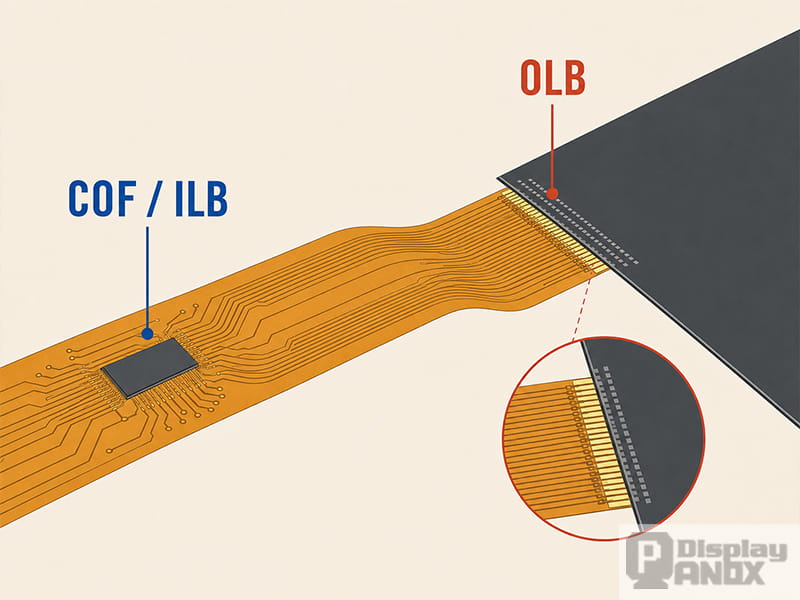
COF bonding and OLB bonding often appear together in LCD module drawings, production records, and factory discussions. The two terms are closely related, but they do not describe the same stage of manufacturing.
COF, or chip-on-film, refers to a packaging structure in which a display driver IC is mounted on a flexible film carrier. OLB, or outer lead bonding, is the module assembly process that connects the outer leads of that COF package to the terminal area of the LCD glass.
A third term, ILB, describes the internal connection between the driver IC and the conductive traces on the flexible film. The relationship can therefore be summarized in one sentence: ILB creates the electrical connection inside the COF package, while OLB connects the completed COF package to the display panel.
COF, ILB, and OLB at a Glance
| Term | Full Name | What It Refers To | Main Connection |
|---|---|---|---|
| COF | Chip-on-Film | An IC packaging method and an intermediate packaged component | Driver IC mounted on a flexible film carrier |
| ILB | Inner Lead Bonding | An interconnection process inside the COF package | IC bumps to the film’s inner leads |
| OLB | Outer Lead Bonding | An LCD module assembly process | COF outer leads to LCD glass terminals, commonly through ACF |
This distinction also explains why the expression “COF bonding” can be ambiguous. In package manufacturing, it may refer to mounting the IC onto the film. On an LCD module production line, the same expression is sometimes used loosely for attaching a prepared COF to the display glass. The technically precise term for the latter operation is OLB, often described in equipment and material documentation as a film-on-glass, or FOG, connection.
What Is COF Bonding?
COF stands for chip-on-film. A bare driver IC is mounted directly onto a flexible carrier film, typically a polyimide film with fine copper circuit patterns. The flexibility of the carrier allows the driver section to fold behind the display panel, helping reduce the border area and overall module thickness.
COF can describe both the packaging technology and the resulting packaged part. From the perspective of LCD module production, a COF is normally an intermediate component: the driver IC has already been mounted, electrically connected, protected, and tested before the film is attached to the display panel.
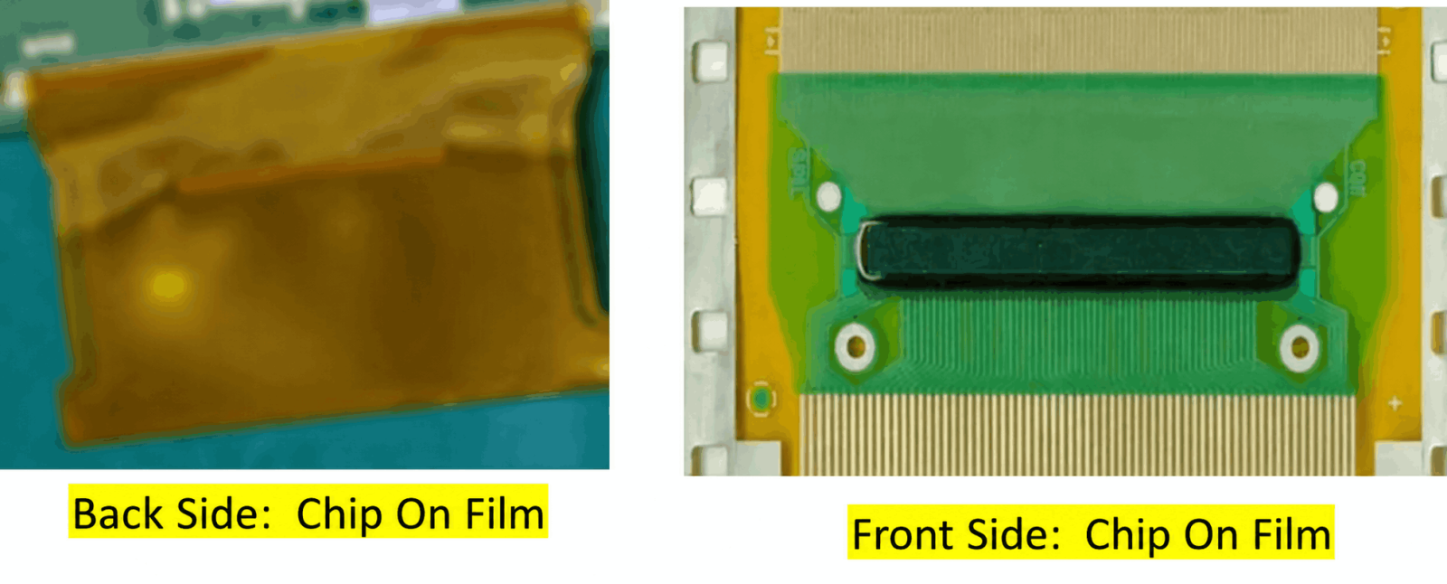
Figure 1. Examples of tape-carrier and COF package structures.
The important point is that COF is not the name of one specific COF-to-glass bonding step. It is the package containing the driver IC, flexible film, circuit traces, and connection leads. The internal chip connection and the external panel connection have their own process names.
How ILB Fits Inside a COF Package
ILB stands for inner lead bonding. During this process, the bumps on the driver IC are joined to the inner copper leads of the flexible film. These connections establish the electrical paths between the IC and the patterned conductors on the COF carrier.
An IEEE study of COF inner lead bonding describes ILB as a thermomechanical process that joins copper inner leads on flexible film to bumps on the driver IC. The bonding method, bump and lead materials, temperature, pressure, planarity, and alignment all affect the strength and electrical performance of the joint.
After ILB, the chip area is normally protected and the packaged COF can be inspected or tested before entering LCD module assembly. An ILB defect is therefore located around the IC-to-film interface rather than at the edge of the LCD glass.
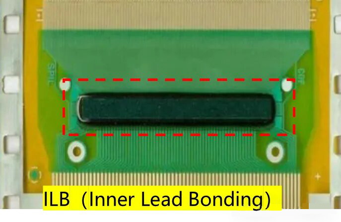
Figure 2. The ILB area between the driver IC and the inner leads of the COF film.
What Is OLB Bonding?
OLB stands for outer lead bonding. Unlike COF, which refers to a packaging structure or component, OLB is a module assembly operation.
During OLB, the panel-side leads extending from the COF film are aligned with the terminal pads along the edge of the LCD glass. These panel terminals commonly include ITO-based or metal electrode structures. An anisotropic conductive film is placed between the two sets of electrodes, after which controlled heat and pressure create the mechanical and electrical connection.
Published research on ACF joints in LCD assembly uses the same process boundary: ILB connects the chip to the film, while OLB connects the COF package to the glass substrate. A display-driver packaging description in US6456353B1 also describes ILB as the IC-to-tape operation followed by OLB between the outer leads and the LCD panel terminals.
In practical terms, OLB is the connection visible along the glass edge after the COF has been mounted.
OLB Viewed from the Side
From the side, the OLB region consists of the COF lead pattern, ACF layer, and terminal area on the LCD glass. The bonding head applies the required heat and pressure across this narrow connection zone.
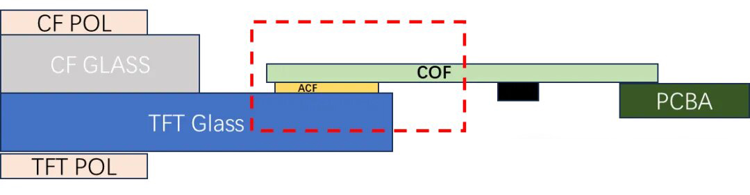
Figure 3. Side view of the OLB connection between the COF and LCD glass.
OLB Viewed from Above
From above, the OLB area appears as a fine-pitch row of aligned leads. Alignment is critical because each COF trace must correspond to the correct panel terminal. Excessive offset can reduce the effective contact area or create a risk of unwanted contact between adjacent circuits.
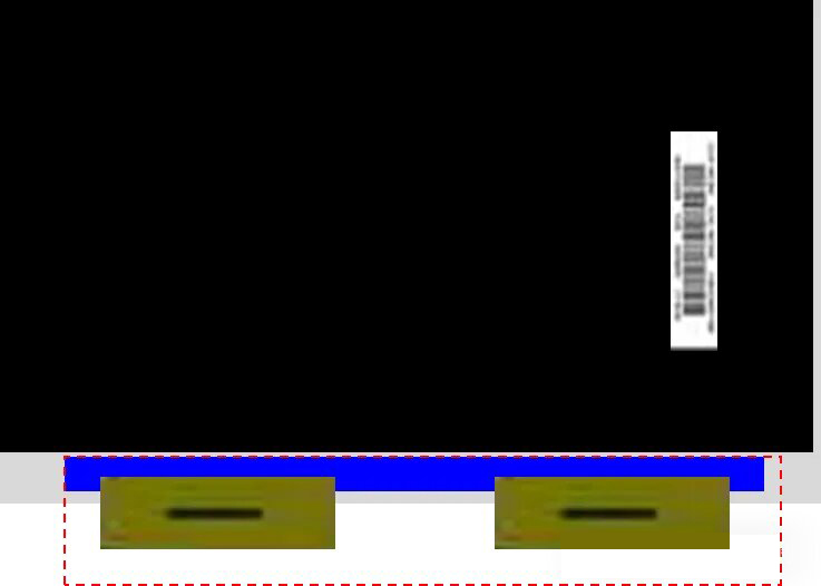
Figure 4. Top view of the OLB bonding area along the LCD glass edge.
How ACF Works in OLB Bonding
ACF stands for anisotropic conductive film. It contains conductive particles dispersed in an insulating thermosetting resin. During thermal compression, particles captured between matching upper and lower electrodes create electrical paths through the thickness of the joint. The surrounding resin retains lateral insulation between adjacent traces.
This directional conduction allows many fine-pitch electrodes to be connected in a single bonding operation. According to Dexerials’ technical explanation of ACF, the general process includes cleaning the connection surface, pre-attaching the ACF, aligning the electrodes, and completing the connection through heat and pressure.
The bonding recipe cannot be treated as a universal set of values. Temperature, pressure, time, ACF construction, electrode pitch, pad material, film thickness, and bonding-head condition must be matched to the specific module design. Incorrect settings may result in high connection resistance, weak adhesion, inadequate particle capture, film deformation, or damaged panel terminals.
Which End of a COF Is Used for OLB?
A typical LCD COF has a panel side and an input side. The panel-side end is bonded to the LCD glass and usually carries a larger number of fine-pitch output traces. The opposite end routes signals and power toward a PCB, FPC, or other driving circuit.
The panel-side copper-based lead pattern is the part used for OLB. These leads may include surface plating and are designed to match the pitch and geometry of the display glass terminals.
Lead count and pitch provide useful visual clues, but the connection drawing should remain the final reference because COF layouts vary between driver ICs and panel designs.
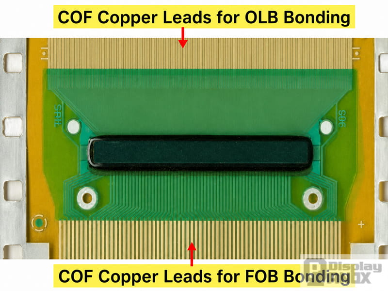
Figure 5. Panel-side COF leads used for the OLB connection.
The Complete COF and OLB Assembly Sequence
The manufacturing sequence becomes clearer when the package stage and module stage are separated.
First, the driver IC bumps are joined to the inner leads of the flexible film through ILB. The protected and tested driver-on-film assembly becomes the COF package. During LCD module assembly, ACF is applied to the glass terminal area, the COF outer leads are aligned with the panel electrodes, and pre-bonding and final thermal compression complete the OLB connection.
The other end of the COF is then connected to the relevant driving circuit according to the module architecture. The panel, driver components, backlight, frame, and other mechanical parts can subsequently be assembled into the finished LCD module.
Bonding, Binding, and Linkage: What Is the Difference?
Although bonding, binding, and linkage all suggest some form of connection, they are not interchangeable in LCD manufacturing.
Bonding is the correct technical term for joining materials or components through heat, pressure, adhesive, conductive particles, or another controlled process. ILB bonding connects the driver IC to the inner leads of the COF film, while OLB bonding connects the COF outer leads to the LCD glass, commonly through ACF.
Binding generally means fastening items together or associating one element with another. It is widely used in software, data processing, and general English, but it is not the standard term for COF, ILB, OLB, or ACF assembly. In display documentation, “COF binding” is usually an imprecise translation of “COF bonding.”
Linkage describes a connection or functional relationship between components. It may explain how the driver IC, COF film, and display panel are linked electrically, but it does not identify the manufacturing process used to create that connection.
For LCD module documentation, bonding should therefore be used for the assembly process, while connection, interconnection, or linkage may be used when describing the resulting electrical relationship.
Why the Difference Matters in LCD Module Production
Calling every operation “COF bonding” can create uncertainty between packaging suppliers, panel manufacturers, equipment teams, and module assemblers. A COF package problem may involve the driver IC, film circuitry, or ILB interface, while an OLB problem is located at the COF-to-glass connection.
The distinction also affects equipment and process documentation. An ILB bonder handles the internal chip-to-film connection, whereas an OLB pre-bonding or main-bonding machine handles the external connection to the panel. Inspection criteria, bonding parameters, failure locations, and rework possibilities are different.
For Panox Display projects, the clearest description identifies both the component and the interface: “COF package with completed ILB” for the packaged driver component, and “ACF-based OLB between the COF and LCD glass” for the panel assembly step.
Conclusion
COF and OLB are related, but they are not the same concept. COF, or chip-on-film, is an IC packaging technology and an intermediate driver component. ILB forms the internal connection between the driver IC and the flexible film. OLB then connects the outer leads of that COF package to the LCD glass, commonly through ACF thermal compression.
In LCD module documentation, bonding is the correct technical term for manufacturing operations such as ILB, OLB, and ACF bonding. Binding is not normally used for these assembly processes, while linkage describes a functional or electrical relationship rather than the process used to create it. Using COF, ILB, OLB, and bonding precisely helps distinguish package construction from module assembly and makes equipment, process, and defect descriptions clearer.