







MIPI DSI is widely used in smartphones and other high-resolution display systems, but many embedded products do not need that level of bandwidth or integration complexity. For compact LCD and OLED modules controlled by a microcontroller, an SPI display remains a practical and cost-effective option.
SPI displays can handle text, graphics, menus, static images, charts, and carefully designed animations. Their main limitation is not image quality, but the time required to transfer every changed pixel through a single serial data path. Understanding that bandwidth limit makes it easier to decide whether SPI is sufficient or whether a faster interface such as MIPI DSI is required.
What Is an SPI Display?
SPI stands for Serial Peripheral Interface, a synchronous serial communication interface commonly used between microcontrollers and peripheral devices. Data transmission is synchronized by a clock generated by the host. A conventional full-duplex SPI bus uses SCLK, MOSI, MISO, and CS, as described in this SPI interface overview from Analog Devices.
Display modules usually use a write-focused variation. MISO may be omitted if the host does not need to read data from the display, while a display-specific D/C signal is added to distinguish commands from pixel data. As a result, a module advertised as a “4-wire SPI display” often uses the following signals:
| Signal | Function |
|---|---|
| SCLK or SCK | Serial clock generated by the MCU |
| MOSI, SDA, or SDI | Commands and pixel data sent to the display |
| CS | Selects the display controller |
| D/C or DCX | Distinguishes command bytes from display data |
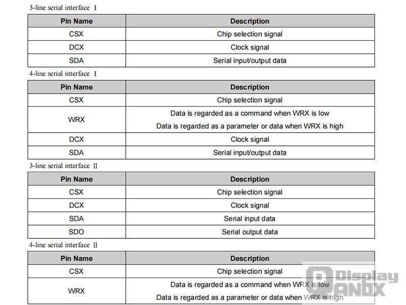
Example ST7789 SPI display interface signals. MISO may be omitted in write-only designs, while D/C distinguishes display commands from pixel data.
The D/C line is part of the display interface implementation rather than standard SPI itself. Reset, backlight control, power, ground, a read-data line, and a TE synchronization signal may also be present, depending on the module.
How Does an SPI Display Work?
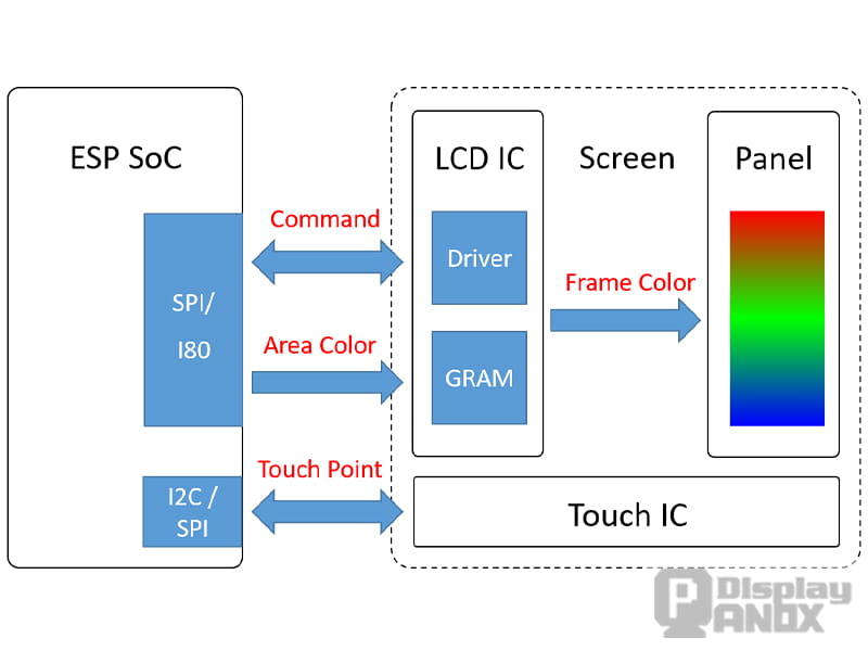
In an SPI LCD, the host transfers commands and changed pixel regions to the controller’s GRAM, while the controller refreshes the panel independently.
Most SPI LCD displays are controller-based MCU displays. The module contains a display driver IC and internal graphics memory, usually called GRAM or frame memory.
The MCU first sends initialization commands to the display controller. When the image changes, it defines a drawing window and transmits the required pixel data through SPI. The controller stores those pixels in GRAM and scans the stored image to the LCD or OLED panel using its own timing circuits.
For example, the ILI9341 controller specification describes an integrated 240 × 320 × 18-bit graphics RAM. Espressif also distinguishes controller-based LCDs by noting that their frame buffer is located inside the display controller rather than necessarily inside the host MCU in its LCD programming documentation.
This architecture has an important advantage: once an image has been written to GRAM, the MCU does not need to retransmit it continuously just to keep it visible. However, every changed pixel still has to cross the SPI bus, which becomes the main performance bottleneck during full-screen animation.
What Can an SPI Display Show?
An SPI display can present text, numbers, symbols, icons, menus, buttons, status indicators, and other embedded UI elements. Static photographs and illustrations are also possible as long as the module supports the required color format and the MCU has enough storage or decoding capacity.
Charts, waveforms, progress bars, timers, and simple animations generally work well because only part of the image changes at a time. Small moving objects can also appear smooth when the firmware redraws only their previous and current positions.
The limitation becomes more visible when most of the screen changes in every frame. Full-screen page transitions, fast scrolling, complex touch animations, and video require a much larger stream of pixel data. Small SPI screens can technically display low-resolution video under carefully optimized conditions, but conventional SPI is rarely the best interface for sustained, full-screen video playback.
How Fast Can an SPI Display Refresh?
The theoretical transfer time for one full frame can be estimated from the resolution, transferred bits per pixel, and SPI clock:
Frame payload = width × height × transferred bits per pixel
Ideal full-frame transfer time = frame payload ÷ SPI clock frequency
Ideal full-frame rate = SPI clock frequency ÷ frame payload
For a 240 × 240 display using RGB565 at a hypothetical 40 MHz SPI clock:
240 × 240 × 16 = 921,600 bits
921,600 ÷ 40,000,000 = 0.02304 seconds
The ideal result is approximately 23 milliseconds per frame, or 43 full frames per second.
That figure assumes that every clock cycle carries useful pixel data. A real system also spends time setting the drawing window, sending commands, rendering the UI, preparing buffers, switching transactions, and waiting for the display or shared bus. Depending on the MCU and driver implementation, the same system may deliver closer to 20 frames per second during continuous full-screen updates.
The effect of increasing resolution is easy to see:
| Resolution | RGB565 Frame Payload | Ideal Transfer Time at 40 MHz | Ideal Maximum Full-Frame Rate |
|---|---|---|---|
| 240 × 240 | 921,600 bits | 23.0 ms | 43.4 fps |
| 320 × 240 | 1,228,800 bits | 30.7 ms | 32.6 fps |
| 320 × 480 | 2,457,600 bits | 61.4 ms | 16.3 fps |
| 480 × 800 | 6,144,000 bits | 153.6 ms | 6.5 fps |
These figures are theoretical and do not guarantee that a particular display controller is rated for a 40 MHz clock.
It is also important to separate the panel scan rate from the host update rate. A panel controller may scan its internal memory at 60 Hz while the MCU can replace only 20 complete frames per second through SPI. In that situation, the panel is still scanning normally; the SPI transfer is limiting how quickly new content reaches its memory.
What Determines SPI Display Performance?
SPI Clock Frequency
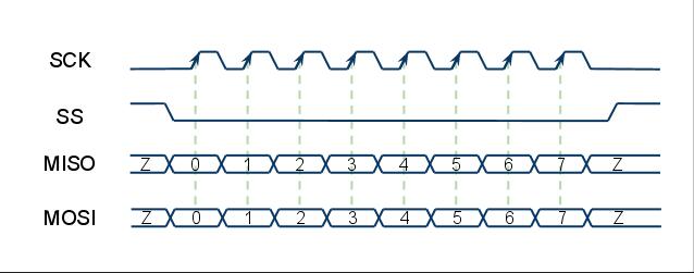
Simplified SPI timing showing clock-synchronized serial data transmission.
SPI does not define one universal maximum clock for every display. The limit depends on the display controller, MCU peripheral, module layout, cable or FPC length, voltage, and signal integrity.
Published controller specifications illustrate this variation. The ST7789V datasheet specifies a minimum 66 ns serial write cycle for its four-wire interface, equivalent to approximately 15.2 MHz. The ILI9341 specification lists a 100 ns minimum write cycle, equivalent to 10 MHz. Other controllers and qualified modules may support higher rates.
A host MCU may offer 40, 60, 80, or even 100 MHz and above as selectable SPI settings, but that does not mean the connected screen supports those frequencies. Espressif’s official SPI LCD guidance similarly states that the configured pixel clock should remain within the range recommended by the LCD specification.
Operating beyond the rated timing may appear to work during a short test but can produce corrupted pixels, intermittent failures, temperature-dependent instability, or poor production yield. High clock settings should therefore be verified with the complete module and PCB rather than treated as a universal SPI capability.
Pixel Format and Transferred Color Depth
RGB565 is widely used because it provides 65,536 colors with only 16 transferred bits per pixel. It is often the best balance between visual quality, memory use, and refresh speed for an MCU-driven display.
RGB666 provides more color information, but its transfer cost depends on the controller protocol. A tightly packed 18-bit transfer contains 12.5% more data than RGB565 and lowers the theoretical frame rate by about 11%. Some byte-oriented controllers send RGB666 as three bytes per pixel, increasing the transfer payload to 24 bits and reducing performance more substantially.
An 8-bit color mode can theoretically double the transfer rate compared with RGB565 if the display controller accepts a true 8-bit pixel format. The trade-off is a smaller color palette and more visible banding. Supported pixel formats and their wire encoding must always be confirmed in the controller datasheet.
Full-Screen and Partial Refresh
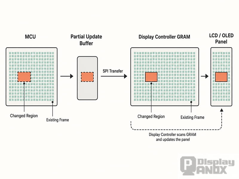
Partial SPI display update.
Update strategy often matters more than raw clock frequency. A full-screen refresh transmits every pixel, even when only one number or icon has changed. A partial refresh defines a smaller address window and sends data only for that region.
At 40 MHz, updating a 40 × 80-pixel RGB565 area requires only 51,200 bits, giving an ideal transfer time of about 1.28 milliseconds. This is why sensor values, timers, progress bars, and local indicators can respond quickly even when the same display feels slow during a full-screen transition.
Embedded graphics libraries can automate this approach. The LVGL display documentation explains that partial rendering redraws only the affected area, while full-screen refreshes over a serially connected external controller are generally too slow for high frame rates.
DMA, Buffering, and Driver Efficiency
DMA does not increase the physical bandwidth of the SPI bus, but it can reduce pauses between transfers and allow the MCU to render the next area while the current buffer is being transmitted.
Long, continuous transfers are generally more efficient than sending pixels through many small function calls. Hardware SPI, DMA, double buffering, cached graphics, and compact drawing regions can therefore make a large difference even when the clock frequency remains unchanged.
Software-generated SPI, inefficient per-pixel drawing functions, repeated command sequences, memory-copy overhead, and a shared SPI bus can reduce the effective frame rate considerably.
TE Synchronization
Some display controllers provide a TE, or Tearing Effect, output. This signal reports the controller’s vertical or horizontal blanking timing so that the MCU can coordinate frame-memory writes with panel scanning.
The ST7789V specification describes the TE signal as a synchronization output used by the host when writing frame memory. Correct use of TE can reduce visible tearing, especially when a large image region is updated.
TE does not make the SPI bus faster. It only helps schedule transfers at a safer point in the panel’s scan cycle. If a full-frame transfer takes longer than the available synchronization window, partial updates or a faster interface may still be necessary.
SPI vs. MIPI DSI Displays
SPI and MIPI DSI are both serial interfaces, but they are designed for different performance levels. The MIPI Alliance defines DSI as a high-speed serial interface between a host processor and a display module. It uses high-speed differential lanes and supports display architectures that require much more bandwidth than conventional single-data-line SPI.
| Design Factor | SPI Display | MIPI DSI Display |
|---|---|---|
| Typical host | MCU with an SPI peripheral | Application processor, SoC, or DSI bridge |
| Data path | Usually one serial pixel-data line | One or more high-speed differential data lanes |
| Integration | Relatively simple firmware and PCB routing | More complex host, initialization, and PHY configuration |
| Best update method | Partial updates to controller GRAM | High-bandwidth command or video transfer |
| Typical content | Text, icons, static UI, local animation | Fluid UI, full-screen animation, and video |
| Common applications | Sensors, appliances, thermostats, compact controls | Smartphones, tablets, handheld terminals, and advanced touch devices |
A practical guideline is to use SPI for small displays with mostly static content, often at resolutions up to approximately 320 × 480. This is not a protocol limit; the acceptable resolution depends on the required frame rate and the percentage of the screen that changes.
For displays at 480 × 800 and above, or products that need smooth full-screen animation, frequent touch scrolling, or video, MIPI DSI is usually the more suitable choice. A broader comparison is available in the Panox Display SPI, RGB, MIPI, and LVDS display interface guide.
Where Are SPI Displays Commonly Used?
SPI displays are well suited to smart home control panels, sensor readouts, compact industrial instruments, small appliances, thermostats, test equipment, and battery-powered devices with low display-update activity.
These applications usually show values, icons, menus, warning messages, and slowly changing graphics rather than continuous video. Their UI can be divided into small independent regions, allowing the firmware to update only what has changed.
SPI can also reduce pin count and simplify the host processor selection. However, low power should not be attributed to the interface alone. The panel technology, backlight, brightness, refresh strategy, and MCU operating state can consume more power than the SPI signals themselves.
What Is the Real Limit of an SPI Screen?
An SPI screen does not have one fixed maximum resolution or frame rate. Its practical limit is determined by the amount of pixel data that must be transferred within the available time.
A compact display with a mostly static interface can deliver responsive performance because only small regions need updating. The same interface can feel slow when every frame replaces hundreds of thousands of pixels. Increasing the SPI clock helps, but it cannot compensate indefinitely for higher resolution, deeper color, and continuous full-screen motion.
For Panox Display projects, interface selection is evaluated together with panel resolution, controller IC timing, pixel format, TE support, host architecture, and the intended UI. SPI is an efficient choice for compact MCU displays with controlled update areas. MIPI DSI is the stronger option when high resolution, smooth interaction, and sustained full-screen bandwidth are central to the product.
Learn more: What Is SPI Interface? How SPI Works?