







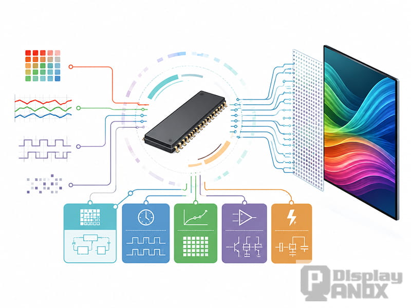
An OLED display driver IC, commonly called an OLED DDIC, sits between the application processor and the display panel. It receives digital image data, interprets display commands, controls scanning timing, processes grayscale values, generates analog driving signals, and manages the power conditions required by the panel.
The DDIC is often described as the “brain” of an OLED display. A modern AMOLED display driver IC may combine functions that were previously handled by several separate components, including the interface receiver, timing controller, frame memory, image-processing pipeline, source driver, gate-control logic, compensation system, and power circuits.
Although the internal design varies by manufacturer and panel architecture, the main responsibilities of an OLED DDIC can be divided into five areas: image interface and protocol parsing, timing control, image processing, pixel driving and compensation, and power management with analog driving. These five areas also form the basic structure of the original article.
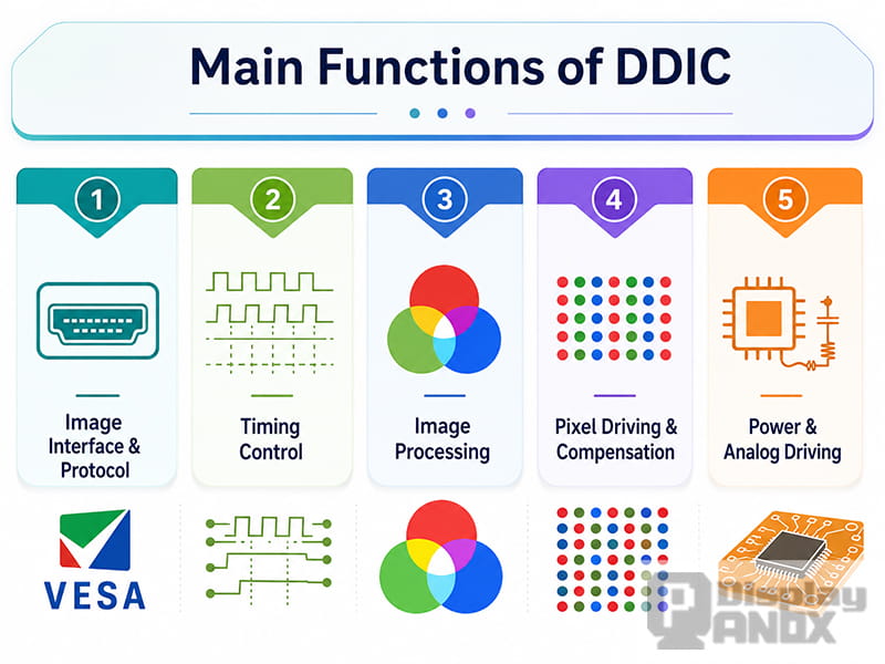
Image Interface and Protocol Parsing
The first task of the DDIC is to receive image data from the application processor and convert the incoming serial signal into an internal image data stream.
In smartphones, wearable devices, handheld terminals, and other compact products, the interface is often MIPI DSI. The application processor sends pixel data and display commands through the MIPI interface. The DDIC receives these packets, checks the data type, interprets the commands, and reconstructs the image information required by the panel.
This process involves more than simply converting serial data into parallel data. The driver must also handle packet boundaries, synchronization, pixel formats, error checking, display commands, and operating-mode changes.
MIPI DSI systems generally support Command Mode and Video Mode. The two modes differ mainly in how image data is transferred and how the panel is refreshed.
Command Mode
In Command Mode, the display driver usually includes display RAM, GRAM, or another local frame-memory structure. Image data sent by the application processor is stored in this memory, and the DDIC reads the stored data to refresh the panel.
Because the panel can retain image data locally, the application processor does not always need to transmit a complete frame continuously. This makes Command Mode useful for static user interfaces, partial-screen updates, wearable products, and low-power applications.
For example, when only a small icon or number changes, the host may update that region instead of resending the entire screen. The DDIC can continue refreshing the remaining image from its internal memory.
The actual behavior still depends on the driver IC and panel design. Not every Command Mode display provides the same frame-buffer capacity, partial-update functions, or self-refresh features.
Video Mode
In Video Mode, the application processor continuously streams pixel data to the display. The DDIC receives the image stream and passes it through the display pipeline according to the timing supplied by the host.
A complete local frame buffer is not always required because the processor continues sending data during active display operation. The DDIC may still contain line buffers, processing buffers, or other temporary memory, but the image is generally treated as a continuous video stream.
Video Mode is suitable for applications in which the host processor manages the complete display timing and continuously provides each frame.
MIPI has continued to expand the interaction between video and command operation. Current DSI specifications support transitions between active video streaming and lower-power command-based operation for static or low-frame-rate content.
VESA Display Stream Compression
High-resolution OLED displays generate a very large amount of image data.
A 1080 × 2400 RGB image with 8 bits for each red, green, and blue channel contains approximately 62.2 Mbit of uncompressed pixel data in one frame. At 60 frames per second, the raw pixel stream reaches about 3.73 Gbit/s before packet overhead, blanking intervals, synchronization data, and control commands are included.
As resolution, refresh rate, and color depth increase, the bandwidth requirement becomes even higher. Some display systems therefore use VESA Display Stream Compression, commonly known as DSC.
When DSC is enabled, the application processor compresses the image before transmission. The DDIC contains a compatible DSC decoder that reconstructs the pixel data before it enters the main image-processing pipeline.
DSC is designed as a low-latency, visually lossless compression system. It can reduce the required interface bandwidth while allowing a display to support higher resolution, higher refresh rates, or greater color depth without simply increasing the number of data lanes.
DSC is not required for every OLED panel. Its use depends on the panel resolution, refresh rate, MIPI lane count, lane speed, pixel format, and the capabilities of both the application processor and the display driver IC. VESA states that DSC is integrated into major display interfaces, including MIPI DSI, and is intended to provide low-latency, visually lossless compression.
Display Timing Control
The timing controller, usually called the TCON, determines when image data is written to the panel and when each row of pixels is selected.
In earlier display architectures, the timing controller could be a separate IC. In many modern mobile OLED and AMOLED products, most timing-control functions are integrated directly into the DDIC.
The timing-control section manages line scanning, frame synchronization, source-data loading, gate-control signals, vertical and horizontal timing, emission timing, and refresh-rate switching. It decides which row is active, when the source driver places data onto the column lines, and when the OLED pixels enter the emission stage.
In Command Mode, the timing controller may read image data from internal display memory and generate a continuous panel-refresh sequence independently of the host. In Video Mode, it remains synchronized with the image stream transmitted by the application processor.
Timing accuracy is critical to display stability. Incorrect porch values, line timing, frame timing, clock settings, or synchronization parameters can cause tearing, flicker, shifted images, horizontal lines, vertical lines, incomplete scanning, unstable refresh, or a completely blank screen.
A panel may receive valid image data and still fail to display correctly if the timing parameters do not match the requirements of the DDIC and panel.
Refresh-rate switching also depends on timing control. When a display changes from 60 Hz to 90 Hz or 120 Hz, the DDIC must adjust the frame period, line timing, data-loading speed, and emission sequence while maintaining stable grayscale and brightness performance.
Image and Grayscale Processing
Modern OLED DDICs usually include an internal image-processing pipeline. Depending on the driver architecture, this pipeline may handle scaling, gamma correction, grayscale mapping, color adjustment, dithering, transition control, low-gray optimization, and panel-uniformity compensation.
Not every image-processing function is completed inside the DDIC. In many high-performance systems, the application processor handles advanced scaling, HDR processing, color-space conversion, and system-level color management. The DDIC then performs the panel-specific corrections required by the physical OLED display.
Scaling
Scaling is required when the resolution of the incoming image does not match the native resolution of the display.
Some DDICs include a basic hardware scaler. This can simplify compatibility with different input resolutions, particularly in cost-sensitive or embedded products.
However, advanced scaling is usually handled by the application processor or display processing unit. The processor normally provides better filtering, more flexible edge processing, and finer control over image sharpness.
For this reason, the built-in scaler of a DDIC may be used as a practical compatibility feature rather than the main image-quality solution in a high-end system.
Gamma Correction
Gamma correction controls the relationship between digital grayscale values and the luminance produced by the OLED panel.
A digital grayscale code does not automatically produce a perfectly linear brightness response. The electrical characteristics of the source driver, pixel transistor, and OLED emitter all affect the final luminance.
The DDIC therefore uses gamma tables, reference voltages, lookup values, or programmable correction curves to convert each grayscale level into an appropriate source-driver output.
Gamma settings influence overall brightness, shadow detail, white balance, color consistency, and the transition between neighboring grayscale levels. Small errors are especially visible in dark images because low-gray levels are separated by very small voltage differences.
Two OLED panels with the same size and resolution may still require different gamma settings. The correct values depend on the OLED material, TFT backplane, pixel circuit, source-driver characteristics, target brightness, and operating temperature.
Color Management
Some OLED DDICs include basic color-adjustment functions, such as color matrices, saturation control, white-point correction, and channel-gain adjustment.
In many modern smartphones and high-performance devices, most advanced color management is handled by the application processor. The host can coordinate display output with operating-system color profiles, HDR content, ambient-light conditions, and different viewing modes.
The DDIC still applies panel-specific adjustments after the main color-processing stage. These adjustments may compensate for differences between the red, green, and blue emitters or correct behavior that is specific to the panel.
Transition Control and Overdrive
Overdrive is most commonly associated with LCD response-time improvement, but some OLED driver systems also include transition-control functions.
These functions adjust the driving value according to the previous grayscale level and the target grayscale level. Their purpose may be to improve transition accuracy, reduce low-gray artifacts, or optimize image behavior at high refresh rates.
The implementation depends on the DDIC manufacturer, OLED material, pixel circuit, and driving method. It should not be assumed that every OLED DDIC uses the same overdrive algorithm or that OLED overdrive works in the same way as LCD overdrive.
Demura Compensation
Mura refers to visible differences in brightness or color across a display panel. It may appear as spots, bands, gradients, cloudy areas, or uneven low-gray regions.
These differences can be caused by variations in TFT characteristics, OLED material deposition, pixel dimensions, electrical resistance, and manufacturing conditions.
Demura compensation corrects the non-uniformity by modifying the grayscale value sent to each pixel or display region. A pixel that is naturally darker may receive a slightly higher corrected value, while a brighter pixel may receive a lower corrected value.
Because every manufactured panel has a different uniformity pattern, Demura calibration is often completed during production testing. The panel displays a series of test images while an optical measurement system records luminance and color differences.
The resulting correction data can be stored in flash memory, OTP memory, EEPROM, or another nonvolatile memory area associated with the display module.
When the display powers on, the calibration data is loaded into the DDIC’s internal Demura RAM. The image-processing pipeline then uses the data to correct the grayscale values before they reach the source driver.
Research on OLED Demura describes the process as a way to compensate for production-related luminance and chromaticity variation by adjusting the grayscale values applied to different pixels.
OLED Pixel Driving and Compensation
Pixel driving and compensation are among the most difficult and important parts of an OLED display driver system.
An AMOLED pixel normally contains an OLED light-emitting element, a driving thin-film transistor, switching transistors, and one or more storage capacitors. The data voltage written by the source driver determines the current that flows through the OLED during the emission period.
In practice, the relationship between data voltage and OLED luminance is affected by driving-TFT threshold-voltage variation, carrier-mobility variation, OLED aging, temperature, panel resistance, manufacturing differences, and electrical crosstalk.
Without compensation, pixels receiving the same digital grayscale value may not produce the same brightness.
Threshold-Voltage Variation
The threshold voltage of the driving TFT can vary between pixels. It may also shift as the panel operates over time.
When the threshold voltage changes, the same source-driver voltage can produce a different OLED current. The resulting luminance difference is particularly noticeable at low grayscale levels.
AMOLED pixel circuits may use internal compensation methods to detect or cancel the threshold-voltage variation. The DDIC may also apply external correction based on calibration data or measured panel behavior.
The goal is to keep the OLED current close to the intended value even when the electrical characteristics of the driving transistor are not perfectly uniform.
Published AMOLED pixel-circuit research frequently focuses on compensating threshold-voltage and mobility variations because these factors directly affect current accuracy and display uniformity.
OLED Aging
OLED materials gradually change during operation. The aging rate is affected by brightness, current density, temperature, displayed color, and accumulated operating time.
Pixels that display bright static content for long periods may age faster than surrounding pixels. This can produce image retention, brightness differences, or permanent burn-in.
Some OLED systems use compensation algorithms to estimate or measure this degradation. The driving values can then be adjusted to reduce the visible difference between aged and less-used pixels.
Compensation cannot completely prevent material aging, but it can improve luminance consistency and extend the period during which the panel maintains acceptable image quality.
IR Drop Compensation
IR drop is caused by electrical resistance in the power lines and metal routing inside the OLED panel.
When a large bright image is displayed, the panel’s current demand increases. The voltage available to different pixels may then vary according to their position and distance from the power connection.
For example, when a full-white image is displayed, pixels near the IC or power input may appear brighter than pixels farther away. The voltage drop accumulates along the power line, causing different areas of the panel to operate under different electrical conditions.
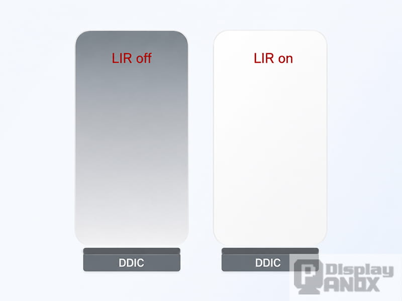
To reduce this problem, the DDIC may apply position-based or image-load-based compensation. The correction value can vary according to pixel position, expected current demand, and the electrical characteristics of the panel.
IR drop compensation is particularly important for larger OLED panels, high-brightness operation, and images containing large bright areas.
Crosstalk Compensation
Crosstalk occurs when the electrical condition of one pixel, row, column, or image area affects another.
It may be caused by parasitic capacitance, shared power lines, line resistance, insufficient charging time, or interaction between scanning and emission periods.
The visible result may include brightness variation, shadowing, line artifacts, or changes in nearby pixels when the image content changes.
OLED DDICs may reduce crosstalk through waveform control, timing optimization, load-dependent correction, and panel-specific compensation algorithms.
Because crosstalk is closely related to the panel structure, a compensation method developed for one panel may not work correctly with another panel, even when both displays have the same size and resolution.
Power Management and Analog Driving
The power and analog section is one of the most technically demanding parts of an OLED DDIC.
The driver does more than process digital image data. It must also generate precise analog voltages across hundreds or thousands of source channels while maintaining low noise, stable references, accurate timing, and consistent output between channels.
Small errors in voltage, linearity, settling time, or reference stability can become visible as grayscale differences, color errors, flicker, or non-uniform brightness.
Source Driver DAC
The source-driver digital-to-analog converter converts the corrected digital grayscale code into an analog data voltage.
This voltage is sent through the source or data line to the selected pixel circuit. The pixel circuit stores the programmed value and uses it to control the OLED current during the emission period.
The accuracy of the source-driver DAC directly affects grayscale performance. Poor channel matching, nonlinearity, slow settling, or electrical noise can create visible differences between columns or neighboring grayscale levels.
The DAC must also settle within the available line time. As the refresh rate or horizontal resolution increases, the time available to program each row becomes shorter.
Gamma Reference
The gamma-reference circuit provides a set of stable reference voltages used by the source-driver DAC.
These reference levels define how digital grayscale codes are converted into analog output voltages. Programmable gamma settings can be used to adjust luminance response, white balance, low-gray behavior, and panel-to-panel variation.
The gamma-reference system must remain stable across temperature, brightness settings, and power conditions. Reference noise or drift can affect the entire display because the same voltage structure is shared by many source channels.
Charge Pumps, Regulators, and Power Circuits
OLED panels require several power rails that may not be supplied directly by the application processor.
The DDIC or an associated power-management IC may contain charge pumps, DC-DC converters, low-dropout regulators, level shifters, current-bias circuits, and voltage-reference generators.
These circuits provide the positive and negative OLED power rails, gate voltages, source-driver references, digital logic supplies, and other panel-specific voltages.
Power sequencing is also important. The different voltage rails must be enabled and disabled in the correct order. Incorrect sequencing can cause unstable startup, flicker, abnormal brightness, image artifacts, or long-term panel stress.
Power ripple, insufficient current capacity, and unstable reference voltages can also affect display performance even when the digital interface and initialization commands are correct.
Typical OLED DDIC Architecture
A simplified OLED DDIC can be divided into a digital data path, timing-control path, analog-driving path, memory system, and power system.
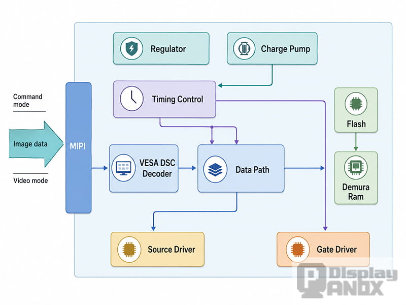
The image data path begins at the application processor. MIPI DSI data enters the interface receiver and passes through the protocol decoder. When DSC is used, the compressed stream is reconstructed by the DSC decoder.
The image then enters the frame memory or internal data-processing pipeline. Gamma correction, grayscale mapping, low-gray processing, and Demura compensation are applied before the corrected values are sent to the source driver.
The source driver converts the digital grayscale values into analog voltages and sends them to the OLED panel.
At the same time, the timing controller generates the row-scanning, data-loading, and emission timing required by the panel. These control signals are sent to the gate driver or gate-control circuitry so that the correct row is selected when the source data is written.
The power-management section provides the voltage rails and analog references required by the digital logic, source driver, gate driver, and OLED pixel circuit.
Flash Memory and Demura RAM
In a typical OLED module, flash memory may contain calibration data for the individual display panel.
During production, the panel is measured to identify brightness and color differences. The resulting Demura data is written into nonvolatile memory.
When the device powers on, the data is reloaded from flash into Demura RAM. The Demura processing block inside the Data Path uses this calibration information to modify the incoming grayscale values.
After compensation and image processing, the Data Path sends the corrected grayscale values to the Source Driver. The Source Driver converts those values into analog voltages and applies them to the display panel.
At the same time, the Timing Control block sends the required timing logic to the Gate Driver. This ensures that each row is selected at the correct moment and that the source voltage is written into the correct pixel circuit.
This simplified sequence explains the relationship between Flash, Demura RAM, Data Path, Source Driver, Timing Control, and Gate Driver. The actual internal structure is considerably more complex, but these blocks describe the main path from image input to pixel output.
Other Internal DDIC Modules
A practical OLED DDIC contains many smaller modules in addition to the main data, timing, and analog blocks.
The OSC block is an internal oscillator used to generate clocks for timing and control functions. The DDIC may use the internal oscillator during startup, low-power operation, or display-refresh modes that do not rely entirely on an external clock.
OTP, or one-time programmable memory, stores panel settings, trimming values, identification data, gamma parameters, voltage settings, and other information that should remain fixed after production.
LVD, or low-voltage detection, monitors the supply voltage and helps prevent unstable operation when the voltage falls below a safe level.
The DDIC may also contain register banks, built-in self-test functions, electrostatic-discharge protection, tearing-effect control, temperature-compensation logic, error monitoring, and diagnostic circuits.
Some products integrate display and touch control into a single device. These components are commonly called touch and display driver integration ICs, or TDDIs.
Why the OLED DDIC Matters in Display Selection
Panel size and resolution provide only part of the information required for display integration. The driver IC determines many of the electrical and software requirements of the final product.
A display must match the host processor’s interface, lane configuration, pixel format, operating mode, and supported transmission speed. The initialization commands, reset sequence, power rails, refresh-rate settings, gamma parameters, and sleep behavior must also match the DDIC.
Two OLED panels can have the same resolution and connector pin count but still be incompatible. They may use different driver ICs, MIPI timings, initialization tables, voltage levels, power sequences, or DSC parameters.
The DDIC also affects partial updates, self-refresh, tearing-effect synchronization, low-power modes, brightness control, display orientation, color depth, and supported refresh rates.
For this reason, the DDIC model and initialization specification should be reviewed together with the panel drawing and electrical specification.
Panox Display’s Approach to OLED Integration
Panox Display evaluates the OLED panel and its display driver IC as one complete display system.
A suitable display solution must match the mechanical dimensions, resolution, brightness, interface, refresh rate, power requirements, touch structure, cover glass, host platform, and final application.
DDIC compatibility is reviewed together with the MIPI timing, initialization sequence, reset behavior, power sequence, FPC definition, and controller requirements.
This system-level approach reduces the risk of choosing a panel that appears suitable mechanically but cannot be driven correctly by the target processor or controller board.
For customized projects, the display panel, touch panel, cover glass, FPC structure, and interface solution can also be evaluated together instead of being treated as unrelated components.
Conclusion
The OLED display driver IC connects the digital image-processing system to the physical OLED panel.
It receives and decodes image data, controls line and frame timing, applies gamma and panel corrections, compensates for pixel variation, converts grayscale values into analog voltages, and manages the power conditions required for stable display operation.
Its internal architecture directly affects interface compatibility, image quality, refresh rate, power consumption, low-gray performance, brightness uniformity, and long-term panel behavior.
For OLED display integration, the DDIC should be reviewed together with the panel, application processor, power design, software driver, connector, touch structure, and application requirements. A correctly matched DDIC and panel combination reduces display bring-up time and provides a more stable foundation for the complete product.
Frequently Asked Questions
What Does an OLED Display Driver IC Do?
An OLED display driver IC receives image data and commands from the host processor. It manages interface communication, display timing, grayscale processing, pixel compensation, source driving, and panel power control.
Is an OLED DDIC the Same as a Display Controller?
The two terms can overlap, but they are not always identical.
A display controller may refer to the digital processing block inside an application processor, FPGA, or controller board. An OLED DDIC normally includes panel-specific analog source driving, gate control, timing, and compensation functions in addition to digital interface processing.
What Is the Difference Between MIPI DSI Command Mode and Video Mode?
Video Mode continuously streams pixel data from the host processor to the display.
Command Mode normally stores image data in local display memory and allows the DDIC to refresh the panel from that stored data. Command Mode may also support partial-screen updates and lower-power operation for static content.
Why Does an OLED Display Need Pixel Compensation?
OLED luminance can be affected by TFT threshold-voltage variation, mobility differences, OLED aging, temperature, IR drop, manufacturing variation, and electrical crosstalk.
Compensation adjusts the driving values to reduce the resulting brightness and color differences.
What Is Demura in an OLED Display?
Demura is a calibration and correction process used to reduce panel brightness and color non-uniformity.
The panel is measured during production, and correction data is generated for different pixels or display regions. The DDIC uses this data to modify the grayscale values before they are sent to the source driver.
Does Every OLED DDIC Support DSC?
No. DSC support depends on the DDIC, panel resolution, refresh rate, interface bandwidth, lane configuration, and target application.
The application processor and DDIC must both support compatible DSC settings.