







MIPI DSI display bring-up is often described as a register-configuration task. In practice, it is a chain of engineering decisions that begins with the panel specification and ends only when the display produces a stable image across temperature, voltage, startup, suspend, and resume conditions.
A working configuration must align three sources of truth:
- The MIPI DSI and D-PHY protocol rules define what the link can do.
- The SoC or MCU documentation defines how the DSI host and PHY must be configured.
- The panel datasheet defines what the specific display module accepts.
The panel specification takes priority whenever a generic recommendation conflicts with a device-specific requirement.
A reliable bring-up process follows this path:
Panel specification → transfer mode → bandwidth calculation → packet configuration → panel initialization → first frame → stability validation
This guide develops that complete path for conventional MIPI DSI displays using D-PHY. It focuses on Video Mode, Command Mode, DCS commands, lane-rate calculation, panel initialization, readback, first-frame validation, and systematic troubleshooting. For a broader comparison with SPI, RGB, and LVDS, see the display interface selection guide.
1. Why MIPI DSI Display Bring-Up Is Difficult
A MIPI DSI display can remain black even when most of the system is working.
The panel may have valid power but still be held in reset. The D-PHY PLL may be locked while the panel remains in Sleep Mode. Low-power commands may work while the high-speed video stream is unstable. The framebuffer may contain a correct image, but the panel may interpret RGB888 data as RGB666. A backlight can turn on even when the display controller has never received a valid frame.
These failures look similar from the outside because the display itself provides very little diagnostic information. The screen may be black, white, shifted, noisy, or intermittently unstable, but each symptom can originate at several different layers.
The fastest way to bring up a new MIPI DSI panel is therefore not to change several registers at once. It is to make each layer produce evidence before moving to the next one.
A useful engineering sequence is:
- Confirm the panel specification and board wiring.
- Validate power and reset timing.
- Start the DSI host and D-PHY without video.
- Prove low-power command communication.
- Perform readback when the panel supports it.
- Send the approved initialization sequence.
- exit Sleep Mode and enable the display.
- Transmit a solid-color frame.
- Test geometry and pixel packing.
- Monitor ECC, CRC, FIFO, PHY, and timeout errors.
- Enable dynamic content.
- Add low-power and performance optimizations one at a time.
This sequence reduces the number of variables at every stage.
2. The Three Layers of a MIPI DSI Display Link
Many confusing explanations mix panel commands, packet structure, and electrical signaling as though they were the same subject. A practical design keeps them separate.
2.1 Application and display-control layer
The upper layer includes:
- MIPI Display Command Set, or DCS
- Generic commands
- Panel initialization
- Sleep and display-state control
- Address-window programming
- Tearing-effect synchronization
- Brightness or backlight control
Commands such as 0x11 Sleep Out and 0x29 Display On belong to this layer.
2.2 DSI protocol layer
The protocol layer defines how information is placed into packets. It includes:
- Short and Long Packets
- Data Type, or DT
- Virtual Channel, or VC
- Word Count
- Header ECC
- Payload CRC
- Video packet sequencing
- Read responses and error reports
This layer answers questions such as whether a command is sent as a DCS Short Write, DCS Long Write, Generic Write, or Read Request.
2.3 D-PHY physical layer
The physical layer includes:
- High-Speed and Low-Power signaling
- Clock Lane and Data Lanes
- Stop State
- Start-of-Transmission and end-of-transmission behavior
- Bus Turn-Around
- ULPS
- Lane timing and electrical margin
The distinction matters because similar names can describe unrelated concepts.
For example:
0x11 Sleep Outis a DCS command, not a D-PHY state.- ULPS is an electrical low-power state, not panel Sleep Mode.
- CRC errors indicate corrupted Long Packet payloads, not necessarily a bad framebuffer.
- HS and LP describe physical signaling, while Short and Long describe packet structure.
A more detailed overview of these layers is available in the Panox MIPI DSI interface guide.
3. How a Frame Travels Through MIPI DSI
Before calculating lane rate, the display scanning model must be separated from the DSI transfer model.
A conventional parallel RGB interface presents a continuous pixel clock, horizontal and vertical synchronization, data enable, and parallel RGB values. MIPI DSI serializes the same display information into packets and sends it through one or more high-speed data lanes.
The display timing still exists even though the link no longer exposes a traditional parallel RGB bus.
3.1 Horizontal and vertical timing
One horizontal line contains four regions:
|<-- HSA -->|<-- HBP -->|<------ HACT ------>|<-- HFP -->|
One frame contains the corresponding vertical regions:
| VSA | VBP | VACT | VFP |
The parameters mean:
| Parameter | Meaning | Contains visible pixels |
|---|---|---|
| HSA | Horizontal Sync Active | No |
| HBP | Horizontal Back Porch | No |
| HACT | Horizontal Active Area | Yes |
| HFP | Horizontal Front Porch | No |
| VSA | Vertical Sync Active | No |
| VBP | Vertical Back Porch | No |
| VACT | Vertical Active Area | Yes |
| VFP | Vertical Front Porch | No |
The totals are:
HTOTAL = HSA + HBP + HACT + HFP
VTOTAL = VSA + VBP + VACT + VFP
Porch and sync intervals should not be reduced merely because they do not contain visible pixels. They can be required by the panel timing controller, source driver, gate driver, or internal scanning architecture.
When a datasheet provides minimum, typical, and maximum values, the typical values are normally the safest starting point. If only the active resolution is known, the missing porch and sync values cannot be derived uniquely.
Two displays with the same resolution may require different timing.
4. MIPI DSI Video Mode vs. Command Mode
The choice between Video Mode and Command Mode changes the transfer model, bandwidth calculation, synchronization method, and power strategy.
4.1 Video Mode
In Video Mode, the host continuously supplies a rasterized stream that corresponds to the panel timing. The display normally does not depend on a complete internal frame buffer for image retention.
A simplified active line may look like this:
H Sync Event
    ↓
Horizontal Blanking
    ↓
RGB Pixel Long Packet
    ↓
Horizontal Blanking
Video Mode is commonly used for LCDs and other panels that expect a continuous stream.
4.2 Command Mode
Command Mode usually relies on display memory inside the panel driver IC. The host configures an address window and writes pixels into panel GRAM:
DCS 0x2A → Set Column Address
DCS 0x2B → Set Page Address
DCS 0x2C → Write Memory Start
The panel’s internal timing controller then scans GRAM to the display.
Command Mode is often suitable for:
- Small GUI displays
- Smartwatches and wearables
- Static interfaces
- Partial updates
- Systems that need lower average link activity
Command Mode is sometimes described as having “no timing.” That wording is misleading. It does not continuously serialize a complete DPI raster, but the system must still account for panel scanning, GRAM write speed, TE synchronization, update-window size, and the time available to complete an update.
4.3 The three Video Mode variants
Classic MIPI DSI Video Mode is commonly divided into three forms.
Non-Burst Mode with Sync Pulses
This mode transmits explicit synchronization information, including the sync pulse interval.
A conceptual line is:
HSS → HSA interval → HSE → HBP → RGB → HFP
It is appropriate when the panel requires a more complete representation of the original horizontal sync pulse.
Non-Burst Mode with Sync Events
This mode sends the key synchronization event without necessarily transmitting an explicit end event for every pulse.
A conceptual line is:
HSS → HBP or blanking → RGB → HFP or blanking
The panel reconstructs the required timing from the event and configured display parameters.
Burst Mode
Burst Mode transmits active pixel data at an instantaneous rate higher than the average video requirement. The pixel payload therefore occupies a shorter portion of the line:
|<------ Fast RGB transfer ------>|<------ BLLP or LP ------>|
The remaining time may be used for Low-Power state, other permitted transactions, or reduced PHY activity.
Burst Mode does not remove porch timing. It compresses the active pixel transfer into a shorter time. The selected lane rate must therefore be high enough to create the intended idle interval.
4.4 Non-Burst does not mean “always HS”
A common oversimplification states that Non-Burst Mode must remain in High-Speed state throughout blanking, while Burst Mode always returns to Low-Power state.
Actual behavior depends on the host controller, panel capability, and available transition time. A Non-Burst implementation may represent blanking with Blanking Packets or Null Packets, but some systems can enter LP during suitable intervals.
The more useful distinction is:
- Non-Burst sends pixels at a cadence closely related to display scanning.
- Burst sends pixels faster than the average requirement to create a longer idle interval.
4.5 Continuous and non-continuous Clock Lane operation
With a continuous clock, the Clock Lane remains active in HS mode even when there is no active payload. This usually simplifies early bring-up and avoids repeated Clock Lane transitions.
With a non-continuous clock, the Clock Lane may return to Stop State, typically LP-11, during suitable idle periods. This can reduce power but places more pressure on PHY timing and panel compatibility.
For initial bring-up, continuous clock is often the more controlled starting point when the panel supports it. Non-continuous clock can be enabled later as a separate optimization.
5. MIPI DSI Lane Rate Calculation
The bandwidth calculation should begin only after the panel timing, pixel format, lane count, and operating mode are known.
At minimum, the input table should contain:
| Category | Required information |
|---|---|
| Panel timing | HACT, HSA, HBP, HFP, VACT, VSA, VBP, VFP and refresh rate |
| Pixel format | RGB565, packed RGB666, loosely packed RGB666, RGB888 or another supported format |
| DSI configuration | Video or Command Mode, Video Mode subtype, lane count, VC and clock behavior |
| Panel limits | Minimum and maximum per-lane rate |
| Host limits | Supported lane count, PLL range, PHY range, packetizer rules and FIFO constraints |
Panox provides a focused explanation of the relationship between bandwidth and lane count in MIPI DSI Data Lanes: How Many Does a Display Need?.
5.1 Step 1: calculate the pixel clock
For Video Mode:
PCLK = HTOTAL × VTOTAL × FPS
Consider an instructional panel with these parameters:
HACT = 800
HSA  = 10
HBP  = 20
HFP  = 20

VACT = 1280
VSA  = 2
VBP  = 8
VFP  = 8

FPS  = 60
The totals are:
HTOTAL = 800 + 10 + 20 + 20 = 850
VTOTAL = 1280 + 2 + 8 + 8 = 1298
The pixel clock is:
PCLK = 850 × 1298 × 60
     = 66,198,000 pixels/s
     ≈ 66.198 MHz
The active-pixel rate alone would be:
800 × 1280 × 60
= 61.44 Mpixels/s
That value is lower because it omits horizontal and vertical blanking. Video Mode must satisfy the complete line and frame timing, so the total pixel clock is the correct baseline.
5.2 Step 2: determine the real link bits per pixel
The panel’s nominal color depth does not always equal the number of bits occupied on the DSI link.
| Pixel format | DSI representation | Link occupancy |
|---|---|---|
| RGB565 | 16-bit packed | 16 bits/pixel |
| RGB666 packed | Four pixels in nine bytes | 18 bits/pixel |
| RGB666 loosely packed | Three bytes per pixel | 24 bits/pixel |
| RGB888 | Three bytes per pixel | 24 bits/pixel |
Loosely packed RGB666 is a frequent source of calculation errors. It contains 18 meaningful color bits, but each pixel occupies three bytes on the link.
5.3 Step 3: calculate aggregate bandwidth
For the 800 × 1280 RGB888 example:
Aggregate bandwidth baseline = PCLK × bpp
                             = 66.198 MHz × 24
                             = 1,588.752 Mbit/s
                             ≈ 1.589 Gbit/s
With four Data Lanes:
Minimum average rate per lane
= 1,588.752 Mbit/s ÷ 4
= 397.188 Mbit/s per lane
The theoretical baseline is therefore approximately:
397.2 Mbps/lane
5.4 Why the theoretical minimum is not the final lane rate
The simple formula does not completely represent:
- Packet headers
- Long Packet CRC
- Sync events
- End-of-Transmission packets
- Blanking and Null Packets
- HS-to-LP and LP-to-HS transitions
- Host packetizer restrictions
- FIFO behavior
- Burst compression requirements
- PLL steps
- PHY timing limits
The correct process is:
Theoretical requirement
        ↓
Host-specific bandwidth and timing rules
        ↓
Nearest valid PLL and PHY operating point
        ↓
Panel minimum and maximum lane-rate check
        ↓
Line-time and packetization validation
A fixed 10% or 20% margin is not a protocol rule. Engineering margin should come from the host implementation, PLL choices, panel speed range, D-PHY timing, selected transfer mode, PCB signal integrity, and measured production margin.
5.5 Selecting a practical operating point
Assume that both the host and panel support 500 Mbps per lane. A reasonable initial point for the instructional example is:
Selected lane rate = 500 Mbps/lane
Aggregate capacity = 2.0 Gbit/s
Relative to the 1.588752 Gbit/s theoretical baseline:
2.0 ÷ 1.588752 ≈ 1.259
The selected operating point provides approximately 25.9% capacity above the theoretical baseline.
This does not make 500 Mbps a universal recommendation for every 800 × 1280 display. It is only a valid candidate if the host can generate it, the panel accepts it, the line timer can represent the selected mode, and the D-PHY timing is configured for that rate.
5.6 Lane rate, HS clock and byte clock
These three values must not be confused.
Conventional D-PHY High-Speed signaling uses DDR behavior:
Lane Rate = 2 × HS Clock frequency
For a 500 Mbps lane rate:
HS Clock frequency = 250 MHz
The lane byte clock is:
Byte Clock = Lane Rate ÷ 8
           = 62.5 MHz
Therefore:
| Quantity | Value |
|---|---|
| Lane bit rate | 500 Mbps |
| HS Clock frequency | 250 MHz |
| Lane byte clock | 62.5 MHz |
The exact PLL and divider programming is SoC-specific. A formula from one STM32, NXP, Rockchip, Qualcomm, or other host controller should not be treated as a universal MIPI formula.
5.7 Host and panel speed ranges must overlap
Suppose the calculated minimum is 397 Mbps per lane.
Panel range: 80–1000 Mbps/lane
Host range: 160–1500 Mbps/lane
The usable overlap begins at approximately 397 Mbps and ends at 1000 Mbps.
If the host offers discrete rates of 400, 450, 500 and 600 Mbps, 400 Mbps is too close to the theoretical edge for a comfortable initial configuration. A 450 or 500 Mbps setting may provide a better starting point, provided the host can represent the line timing correctly.
A different system might have:
Panel maximum = 450 Mbps/lane
Lowest stable host setting = 500 Mbps/lane
That system has no valid operating point even if the mathematical payload requirement appears to fit.
5.8 Command Mode bandwidth calculation
Command Mode is better calculated from the amount of data that must be transferred within an available update window.
For a full RGB888 frame:
Frame bits = Width × Height × 24
For a 454 × 454 display:
Frame bits = 454 × 454 × 24
           = 4,946,784 bits
If the entire frame must be written within 14 ms:
Payload bandwidth = 4,946,784 ÷ 0.014
                  ≈ 353.34 Mbps
With two lanes:
Payload rate per lane ≈ 176.67 Mbps/lane
This remains a payload-only baseline. DCS packet overhead, TE behavior, BTA transactions, FIFO limitations, LP/HS transitions, and the actual GRAM write window still matter.
Partial updates can reduce average traffic substantially. A 100 × 100 RGB888 region contains:
100 × 100 × 24 = 240,000 bits = 30,000 bytes
The full 454 × 454 RGB888 frame is approximately 618 KB, so a small regional update can be far less demanding when the panel supports address windows and partial refresh.
6. What MIPI DSI Sends on the Lanes
High-Speed versus Low-Power signaling and Short versus Long Packet format describe different dimensions.
- HS and LP define the D-PHY electrical state.
- Short and Long define the DSI packet structure.
A Short Packet can be transmitted through HS when the host and peripheral permit it. A Long Packet can also be carried through LPDT in supported cases. Pixel streams normally use HS, while a peripheral read response uses the reverse Low-Power path on Data Lane 0.
6.1 Data Identifier
The first packet byte is the Data Identifier:
bit 7  bit 6 | bit 5 ........ bit 0
     VC      |        DT
Therefore:
DI[7:6] = Virtual Channel
DI[5:0] = Data Type
The classic two-bit VC field supports VC0 through VC3.
Data Type identifies the packet as a synchronization event, pixel stream, DCS command, Generic command, read request, response, Blanking Packet, Null Packet, or another defined transaction.
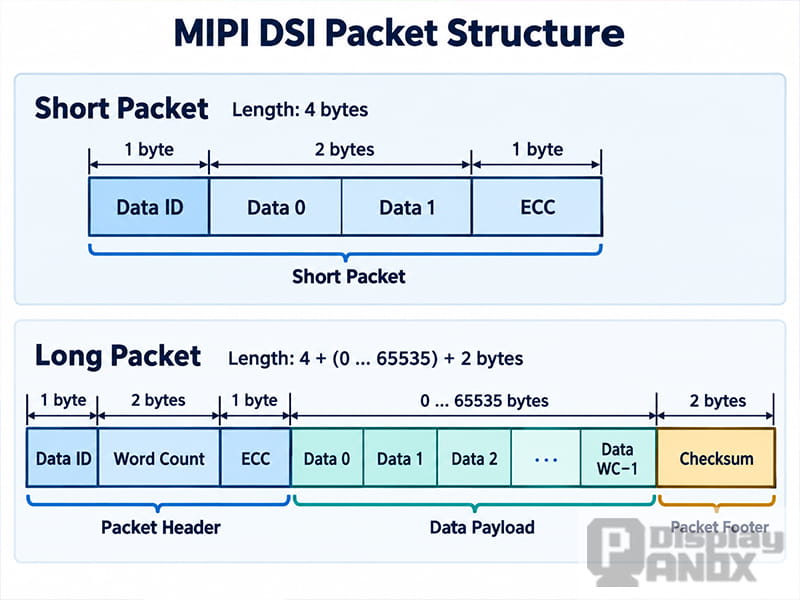
6.2 Short Packet format
A Short Packet is always four bytes:
Byte 0       Byte 1       Byte 2       Byte 3
+-----------+------------+------------+------+
| Data ID   | Data0      | Data1      | ECC  |
+-----------+------------+------------+------+
The meaning of Data0 and Data1 depends on the Data Type.
A DCS Short Write without a parameter uses Data Type 0x05:
Data0 = DCS command
Data1 = 0x00
Sleep Out can therefore be represented as:
DT    = 0x05
Data0 = 0x11
Data1 = 0x00
A DCS Short Write with one parameter uses Data Type 0x15. Setting a common RGB888 pixel format may appear as:
Command   = 0x3A
Parameter = 0x77
The panel documentation must confirm that the format and parameter are supported.
6.3 Long Packet format
A Long Packet contains a four-byte header, payload, and two-byte CRC:
+---------+---------+---------+------+
| Data ID | WC LSB  | WC MSB  | ECC  |
+---------+---------+---------+------+
|                                  |
|              Payload             |
|                                  |
+----------------+-----------------+
| CRC LSB        | CRC MSB         |
+----------------+-----------------+
The total length is:
4 + Word Count + 2 bytes
Word Count is the number of payload bytes. It is not the number of pixels or bits.
For an 800-pixel RGB888 line:
WC = 800 × 3 = 2400 bytes
For RGB565:
WC = 800 × 2 = 1600 bytes
Packed RGB666 groups four pixels into nine bytes. The host may also impose DMA or FIFO alignment rules, but those implementation requirements should not be mistaken for universal DSI packet rules.
6.4 Header ECC and payload CRC
Header ECC protects the first three header bytes:
Data ID + Word Count/Data0 + Word Count/Data1
In the classic packet format, it can correct a single-bit header error and detect a double-bit header error. Multiple-bit errors are not guaranteed to be correctable.
Persistent header ECC errors suggest that the receiver may misinterpret the Data Type, Virtual Channel, Word Count, or command parameters. The investigation should include PHY timing, lane integrity, lane mapping, polarity, clock stability, and speed margin.
Long Packet payloads are followed by a 16-bit CRC. The commonly used polynomial is:
x^16 + x^12 + x^5 + 1
The essential distinction is:
ECC → packet header
CRC → Long Packet payload
CRC detects payload corruption but does not reconstruct the damaged data. CRC errors in pixel packets can appear as colored dots, snow, localized corruption, or damaged lines, depending on how the panel handles a bad packet.
6.5 Reading ECC and CRC patterns
Different error patterns point in different directions.
If both ECC and CRC errors increase, the complete high-speed path may be unreliable. If headers remain clean but CRC errors rise with lane rate or temperature, payload integrity and PHY margin become stronger suspects.
If no ECC or CRC errors appear but the colors are consistently wrong, likely causes include:
- RGB versus BGR ordering
- Pixel format mismatch
- Wrong Pixel Stream Data Type
- Framebuffer format
- Address-mode configuration
- Byte ordering or packing
A clean protocol error register does not prove that the image format is correct.
6.6 Common Processor-to-Peripheral Data Types
| DT | Transaction |
|---|---|
0x01 |
V Sync Start |
0x11 |
V Sync End |
0x21 |
H Sync Start |
0x31 |
H Sync End |
0x08 |
End-of-Transmission Packet |
0x09 |
Null Packet |
0x19 |
Blanking Packet |
0x03 |
Generic Short Write, no parameter |
0x13 |
Generic Short Write, one parameter |
0x23 |
Generic Short Write, two parameters |
0x04 |
Generic Read Request, no parameter |
0x14 |
Generic Read Request, one parameter |
0x24 |
Generic Read Request, two parameters |
0x29 |
Generic Long Write |
0x05 |
DCS Short Write, no parameter |
0x15 |
DCS Short Write, one parameter |
0x06 |
DCS Read |
0x39 |
DCS Long Write |
0x37 |
Set Maximum Return Packet Size |
0x0E |
RGB565 Pixel Stream |
0x1E |
Packed RGB666 Pixel Stream |
0x2E |
Three-byte RGB666 Pixel Stream |
0x3E |
RGB888 Pixel Stream |
A DCS command byte and a DSI Data Type are not the same thing. For example, 0x11 may be the DCS Sleep Out command, while DT 0x05 identifies the packet as a DCS Short Write without a parameter.
6.7 Common Peripheral-to-Processor Data Types
| DT | Return packet |
|---|---|
0x02 |
Acknowledge and Error Report |
0x11 |
Generic Short Read Response, one byte |
0x12 |
Generic Short Read Response, two bytes |
0x1A |
Generic Long Read Response |
0x1C |
DCS Long Read Response |
0x21 |
DCS Short Read Response, one byte |
0x22 |
DCS Short Read Response, two bytes |
A read transaction should be validated by more than the presence of data. The return Data Type, response length, ACK or error bits, Virtual Channel, Maximum Return Packet Size, and BTA status should all be recorded.
6.8 Virtual Channel
Single-panel systems commonly use VC0, but VC0 is not mandatory simply because only one panel is attached.
The requirement is that the host and peripheral use the same Virtual Channel. A host sending VC1 to a panel configured for VC0 can produce a clean electrical link and valid packet checksums while the display ignores every packet.
6.9 EoTp and physical end-of-transmission
The End-of-Transmission Packet uses Data Type 0x08 and belongs to the protocol layer. The D-PHY transition from HS signaling back to LP or Stop State is a physical-layer event.
These should not be treated as the same mechanism. Whether the host sends EoTp may be configurable, so the panel requirement, host documentation, and proven reference design should be checked together.
7. DCS, Generic Commands, Readback, TE, and Low-Power States
7.1 DCS and Generic are not simply “standard” and “private”
DCS defines standardized display-control functions such as Sleep In, Sleep Out, Display Off, Display On, address-window programming, memory write, pixel format, TE control, and status readback.
Generic packets provide a more general transport mechanism.
A real panel initialization table may contain:
- Standard DCS commands
- Manufacturer-defined registers
- Page-select or command-set-unlock sequences
- Generic Short or Long Writes
- Manufacturer commands carried inside DCS Long Writes
A command beginning with 0xB0, 0xB6, or 0xFF cannot be classified from the first byte alone. The Host API, packet Data Type, and panel programming guide must all agree.
7.2 Common DCS commands
| Command | Name | Typical purpose |
|---|---|---|
0x00 |
NOP | No operation |
0x01 |
Software Reset | Reset panel command state |
0x04 |
Get Display ID | Read display identification |
0x09 |
Get Display Status | Read display status |
0x0A |
Get Power Mode | Check sleep and display state |
0x10 |
Enter Sleep Mode | Enter panel low-power state |
0x11 |
Exit Sleep Mode | Wake internal display blocks |
0x28 |
Set Display Off | Disable displayed output |
0x29 |
Set Display On | Enable displayed output |
0x2A |
Set Column Address | Configure the X address window |
0x2B |
Set Page Address | Configure the Y address window |
0x2C |
Write Memory Start | Begin GRAM pixel write |
0x2E |
Read Memory Start | Begin GRAM read where supported |
0x34 |
Set Tear Off | Disable TE output |
0x35 |
Set Tear On | Enable TE output |
0x36 |
Set Address Mode | Configure scan, mirror or color order |
0x3A |
Set Pixel Format | Configure panel pixel format |
0x3C |
Write Memory Continue | Continue a GRAM write |
0x44 |
Set Tear Scanline | Configure a TE scanline |
Panel support and parameter encoding must always be confirmed.
7.3 Pixel format is an end-to-end contract
Changing only one pixel-format setting is not sufficient. The complete chain may contain:
Framebuffer format
        ↓
Display controller input format
        ↓
DSI host pixel format
        ↓
Pixel Stream Data Type
        ↓
Panel DCS pixel format
        ↓
Panel internal format
A mismatch can produce wrong colors, byte misalignment, incorrect line length, repeated pixels, or a completely black display.
Common DCS pixel-format parameters include:
| Format | Common DCS parameter |
|---|---|
| RGB565 | 0x55 |
| RGB666 | 0x66 |
| RGB888 | 0x77 |
These values remain subject to the actual panel implementation.
7.4 Choosing DCS Short or Long Write
A command without a parameter, such as Sleep Out, normally uses a DCS Short Write without a parameter:
DT = 0x05
Command = 0x11
A command with one parameter, such as Pixel Format, normally uses a DCS Short Write with one parameter:
DT = 0x15
Command = 0x3A
Parameter = 0x77
Commands with several parameters, such as a four-byte address range, generally use a DCS Long Write:
0x2A
X start MSB
X start LSB
X end MSB
X end LSB
Some host APIs select the packet format automatically from the buffer length. The actual packet should still be visible in a debug log.
7.5 Reading a panel initialization table correctly
Consider this simplified sequence:
0x11
delay
0x3A, 0x77
0x29
The engineering meaning is:
0x11requests Exit Sleep Mode.- The delay allows internal power, analog, and clock blocks to recover.
0x3A, 0x77configures a supported 24-bit pixel format.0x29enables the display output.
Manufacturer commands should be decoded using the programming guide rather than guessed from their hexadecimal values. They may configure power, gamma, VCOM, gate timing, porch values, lane behavior, or command-page access.
7.6 Initialization delays are functional requirements
Delays may be required for:
- Power-rail stabilization
- Reset pulse width
- Internal startup after reset release
- Recovery after Sleep Out
- Applying manufacturer register changes
- Preparing the panel before Display On
A panel that works with a shortened delay on one bench at room temperature may still fail at cold temperature, high temperature, slow power ramp, low voltage, or on another production lot.
A delay should be reduced only when the panel specification allows it and validation covers process, voltage, and temperature margin.
7.7 A practical power-on state machine
A common structure is:
Enable panel power rails
        ↓
Wait for rails to stabilize
        ↓
Assert RESET
        ↓
Meet minimum reset pulse width
        ↓
Release RESET
        ↓
Wait for internal panel readiness
        ↓
Initialize DSI host and D-PHY
        ↓
Confirm valid Stop State
        ↓
Send LP initialization commands
        ↓
Exit Sleep Mode
        ↓
Wait for the panel-specified delay
        ↓
Apply remaining required settings
        ↓
Set Display On
        ↓
Start video or memory write
        ↓
Enable the backlight
Some panels require the host PHY before reset release, while others define another order. The sequence is a framework, not a universal script.
Keeping the backlight disabled until the first stable frame avoids white flashes, gray screens, and random patterns during initialization. OLED and AMOLED modules may control emission or brightness through panel commands rather than a separate LED backlight, but the same principle applies: visible output should be enabled only after the content path is ready.
7.8 Readback and Bus Turn-Around
A panel read is a complete bidirectional transaction:
Host owns the bus
        ↓
Set Maximum Return Packet Size if required
        ↓
Send DCS or Generic Read Request
        ↓
Initiate Bus Turn-Around
        ↓
Data Lane 0 changes direction
        ↓
Panel returns a packet in reverse LP mode
        ↓
Host receives the packet
        ↓
Panel returns bus ownership
Reverse transfer uses physical Data Lane 0 even when the forward video path uses several lanes.
A successful, repeatable display-ID or power-mode read proves several useful facts:
- The panel is powered.
- Reset is probably released.
- The Host-to-Panel LP path works.
- The command is accepted.
- BTA occurs.
- The panel can transmit on the Lane 0 reverse path.
- The host can receive LP data.
- The protocol and VC are at least broadly aligned.
It does not prove that the high-speed video path works, that all Data Lanes are correct, that the pixel format matches, or that CRC will remain clean.
Some panels do not implement useful readback. Failure to read an ID is therefore not automatic proof of a damaged panel. The display specification must state whether the requested read operation is supported.
7.9 TE synchronization
A Command Mode panel can use the tearing-effect signal to indicate a suitable update point.
A typical chain is:
DCS Set Tear On
        ↓
Panel TE output
        ↓
SoC GPIO interrupt or DSI host TE input
        ↓
Host waits for the event
        ↓
Memory write begins
The design must confirm TE polarity, pulse width, selected TE mode, scan direction, permitted delay after the event, and whether the signal represents only vertical blanking or another synchronization scheme.
Receiving a TE event does not prevent tearing if the host begins a long update too late or cannot finish inside the usable window.
7.10 Display Off, Sleep Mode and ULPS
These are independent states.
Display Off (0x28) disables visible panel output. It does not necessarily remove power or stop DSI communication.
Enter Sleep Mode (0x10) places internal panel circuits into a lower-power state according to the display controller implementation.
ULPS is a D-PHY electrical state for the Clock and Data Lanes. It is not a panel DCS command.
A complete suspend sequence may coordinate all three:
Stop new frame submission
        ↓
Display Off if required
        ↓
Enter Sleep Mode if required
        ↓
Wait for the specified delay
        ↓
Stop HS transactions
        ↓
Enter LP or ULPS
        ↓
Disable power rails if required
Resume reverses the dependency chain. If the panel loses power, its manufacturer registers may also be lost, so resume may require the complete initialization sequence rather than only Sleep Out and Display On.
8. A Minimum-Risk MIPI DSI Bring-Up Procedure
The purpose of bring-up is not merely to run the complete vendor code. It is to reduce uncertainty until each subsystem has passed a clear test.
The Panox practical MIPI DSI bring-up guide provides additional platform and Linux integration context.
Step 0: build a panel fact sheet
Before driver development begins, record:
Power:
IOVCC =
VCI =
AVDD =
AVEE =
Power-on sequence =
Power-off sequence =

Reset:
Active level =
Minimum pulse width =
Delay after release =

DSI:
Lane count =
Lane mapping =
Lane-rate range =
Video or Command Mode =
Video subtype =
Clock mode =
Virtual Channel =
EoTp requirement =

Timing:
HACT =
HSA =
HBP =
HFP =
VACT =
VSA =
VBP =
VFP =
Refresh rate =

Pixel configuration:
Pixel format =
RGB or BGR =
DCS 0x3A requirement =

Control:
Readback supported =
TE supported =
TE polarity =
Sleep Out delay =
Display On sequence =
Backlight or emission control =
If this table cannot be completed, the missing input is documentation rather than code.
Step 1: perform static hardware checks
Check the exact FPC pinout, power rails, RESET, Clock Lane polarity, Data Lane order, backlight path, TE connection, auxiliary GPIOs, and any bridge device.
Confirm that:
Host Lane 0 → Panel Lane 0
Host Lane 1 → Panel Lane 1
Host Lane 2 → Panel Lane 2
Host Lane 3 → Panel Lane 3
Host Clock  → Panel Clock
If a legal lane swap or polarity inversion exists, the host PHY must explicitly support and configure it.
High-speed layout becomes increasingly important as lane rate rises. Routing, impedance, return path, connector transitions, and FPC behavior are covered in the MIPI DSI PCB layout guidelines.
Step 2: verify power and reset only
Keep the backlight or emission path disabled. Measure the actual rail levels and sequencing, then capture reset timing.
The pass conditions are:
- All rails remain within specification.
- The power sequence follows the panel requirement.
- Reset polarity and pulse width are correct.
- The delay after reset release is sufficient.
- There is no abnormal current.
A failure at this stage should remain a power or reset investigation. Changing HFP, HBP, packet size, or lane rate cannot repair an invalid rail sequence.
Step 3: start the DSI host and D-PHY without video
Configure the lane count, provisional lane rate, escape clock, D-PHY timing, Clock Lane policy, and Low-Power command path.
Check the host status for:
- PLL lock
- PHY ready
- Clock Lane Stop State
- Data Lane Stop State
- HS entry or exit errors
- Escape-mode errors
The exact register names differ between host controllers.
Step 4: prove the Low-Power command path
Send a command that the panel documentation clearly supports. Read Display ID or Get Power Mode is valuable when readback is available.
If the panel cannot return data, NOP or Software Reset may confirm that the host can complete a transaction, but a successful transmit return code does not prove that the panel received the command.
The log should include:
Timestamp
Virtual Channel
Data Type
LP or HS mode
Command byte
Payload length
Payload data
Return code
Step 5: validate the reverse path
For a supported read operation, record:
TX Data Type
RX Data Type
RX length
RX payload
ACK/Error Report
BTA timeout
LP RX timeout
A good result has a plausible length, stable repeated value, expected response type, and no BTA or LP receive errors.
Intermittent readback suggests LP timing, Lane 0, power, reset, VC, return-packet-size, or BTA problems.
Step 6: send the approved initialization sequence
The first pass should preserve the vendor command order, transport type, delay, page selection, and payload length.
Each command should be checked immediately:
index
command type
length
first byte
return value
delay
timestamp
If one transaction fails, the sequence should stop at the first meaningful fault. Printing only “initialization complete” after ignoring dozens of return codes removes the most useful evidence.
Step 7: confirm the panel display state
After Sleep Out and Display On, read Get Power Mode or Get Display Status when supported.
Without readback, verify at minimum that:
- The manufacturer initialization sequence completed.
- Sleep Out was transmitted using the correct packet type.
- The required delay was respected.
- Display On was transmitted.
- Video or memory-write operation began in the required order.
Backlight illumination alone does not prove that the panel is ready to display pixels.
Step 8: transmit solid colors
The first image should not be a complex desktop or graphical interface.
Use:
- Full black
- Full white
- Full red
- Full green
- Full blue
Red, green, and blue expose channel order, BGR/RGB swaps, and some pixel-format faults. White makes missing lines, random bit errors, and color noise easy to see. Black helps identify uninitialized regions and separates image-path behavior from backlight leakage.
Step 9: transmit geometry test patterns
Useful patterns include:
| Pattern | Primary purpose |
|---|---|
| Four color quadrants | Channel order, orientation and regional integrity |
| One-pixel border | Active width, active height, cropping and offset |
| Horizontal and vertical lines | Stride, scanning direction and line alignment |
| Checkerboard | Packing, DMA behavior and bit errors |
| Gradient | Color depth, gamma and banding |
| Coordinate labels | Mirror, rotation and address mapping |
A test pattern is a low-cost protocol analyzer for the complete pixel path.
Step 10: check error counters
A visually correct frame is not sufficient.
Run the static patterns for several minutes while monitoring:
- Single-bit and multiple-bit ECC errors
- CRC errors
- FIFO underflow or overflow
- SoT and SoT synchronization errors
- Timeouts
- PLL unlock
- BTA contention
- Video underflow
A display that appears normal while the CRC count rises every second is not ready for production.
Step 11: test dynamic content
After static output is stable, enable continuous framebuffer updates, DMA, page flipping, cache maintenance, animation, and application rendering.
If the DSI host’s internal test pattern is stable while framebuffer output fails, the investigation should move toward memory bandwidth, DMA, cache coherency, display-controller timing, and FIFO underflow rather than immediately blaming the D-PHY.
For Linux systems, platform-level display routing can also be important. The Rockchip DRM/KMS display driver guide illustrates how pixel timing, DRM state, panel binding, and interface bandwidth interact.
Step 12: enable optimizations individually
Only after the baseline is stable should the project add:
- Non-continuous clock
- Burst Mode
- ULPS
- TE synchronization
- Partial refresh
- Higher refresh rates
- Dynamic frequency changes
- Display compression
Each feature should be compared with the known-good baseline while error counters, power, temperature, and resume behavior are monitored.
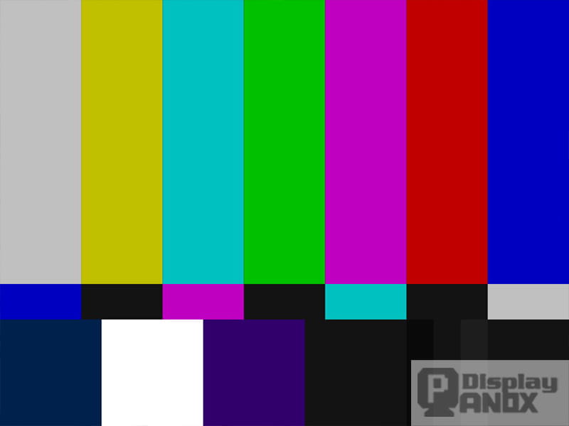
A known test pattern helps verify pixel format, RGB channel order, image alignment, and the integrity of the first stable frame.
9. Systematic MIPI DSI Troubleshooting
A useful fault model divides the display into seven layers:
| Layer | Area |
|---|---|
| L0 | Power and Reset |
| L1 | D-PHY state and PLL |
| L2 | DSI packets, commands and BTA |
| L3 | Panel internal state |
| L4 | Video timing and pixel format |
| L5 | Display controller, DMA and memory |
| L6 | Signal integrity and PVT margin |
The objective is not to claim that every symptom belongs to one layer. The objective is to prevent the investigation from expanding without evidence.
9.1 L0: power and reset
Typical symptoms include:
- No response
- Readback failure
- Intermittent startup
- Cold boot failure with successful warm reset
- Backlight on but no panel state
Check rail voltage, ramp behavior, sequence, reset polarity, reset pulse width, delay after release, and backlight timing.
Useful experiments include extending the reset pulse, extending the power-stabilization delay, and performing a complete power removal instead of a software restart.
9.2 L1: D-PHY and PLL
Check:
- PLL lock
- PHY ready
- Clock Lane Stop State
- Data Lane Stop State
- HS entry and exit errors
- SoT and SoT synchronization errors
- Escape-mode transition errors
Likely causes include the wrong PLL rate, incorrect D-PHY timing, invalid lane count, lane mapping, polarity error, Clock Lane configuration, or a lane rate outside the supported panel range.
PHY register values are implementation-specific. Copying an hs_settle value from another SoC without converting it through the current PHY formula is unreliable.
9.3 L2: packets, LP commands and BTA
Common errors include:
- ECC single-bit or multiple-bit error
- Invalid Data Type
- Invalid Virtual Channel
- BTA timeout
- LP receive timeout
- Protocol violation
- Contention
An invalid Data Type suggests the wrong host packet mode, pixel-stream format, or DCS-versus-Generic API.
An invalid VC requires confirmation that the host and panel use the same Virtual Channel.
A BTA timeout points toward read support, Lane 0, LP receive configuration, panel state, return-packet size, or command timing.
Contention suggests a bus-direction handoff problem.
9.4 L3: panel internal state
A link may complete every transaction without protocol errors while the display remains black.
Confirm that:
- The panel is no longer in hardware reset.
- The manufacturer command page is correct.
- Required power and gamma registers were programmed.
- Sleep Out completed.
- Display On completed.
- Pixel format matches.
- The panel did not return to Sleep Mode.
- Brightness, backlight, or emission control is enabled.
Get Power Mode, Get Display Status, and Get Pixel Format are valuable when supported.
9.5 L4 and L5: timing, format, framebuffer and DMA
Different visual faults provide useful clues.
| Symptom | First checks |
|---|---|
| Entire image shifted | H/V timing, address window and panel offset |
| Every line appears diagonally shifted | Stride, line length, Word Count and packing |
| Red and blue are exchanged | RGB/BGR order and address mode |
| Pixels repeat in a fixed pattern | RGB565/RGB666/RGB888 mismatch |
| Static frame is stable but animation flickers | FIFO, memory bandwidth, DMA and cache |
| Border is clipped | Active dimensions, porch, offset and scaler |
| Fixed horizontal bands | Underflow, line period or timing |
| Gradients show unexpected steps | Color depth, packing and gamma |
A stable internal test pattern with an unstable framebuffer is strong evidence that the DSI link is healthier than the memory-to-display path.
9.6 L6: signal integrity and operating margin
PHY or signal-integrity problems become more likely when:
- Errors increase with lane rate.
- CRC or ECC errors rise at temperature extremes.
- One board behaves worse than another.
- Touching the FPC or connector changes the symptom.
- Lower lane rates improve stability.
- Snow, colored dots, or intermittent flashes appear.
- The same configuration works on a short cable but fails on another mechanical stack.
The investigation should include differential impedance, FPC construction, connector transitions, P/N polarity, lane skew, return path, PHY timing, power noise, and panel speed limits.
9.7 Lane-rate reduction as a diagnostic experiment
Suppose random CRC errors occur at 1000 Mbps per lane. The rate can be tested at 800 and 600 Mbps only if the lower rate still satisfies the video bandwidth, the host timing is recalculated, and the panel supports the new range.
Three outcomes are especially informative.
Errors decrease as the lane rate decreases.
This strongly suggests PHY timing or signal-integrity margin.
The image remains identically misaligned at every rate.
Pixel format, timing, stride, Word Count, or packet configuration is more likely.
The panel goes completely black below a certain rate.
The system may have crossed below the required video bandwidth, the panel or PHY minimum rate, or a valid PLL operating point.
Reducing lane rate is a classification tool. It is not automatically the final solution.
9.8 Other high-value A/B tests
Continuous versus non-continuous clock: If continuous clock is stable while non-continuous clock fails, inspect Clock Lane transitions, PHY timing, and panel support.
Burst versus Non-Burst: A Burst-only failure points toward the burst lane rate, packetization, BLLP timing, or panel mode support.
Internal test pattern versus framebuffer: A stable internal pattern with unstable framebuffer output points toward the display controller, DMA, cache, or memory subsystem.
Cold boot versus warm reset: A cold-only failure increases the priority of power and reset timing.
9.9 Logging that supports diagnosis
A useful startup log records configuration and state rather than printing a generic success message:
[PANEL] power enabled
[PANEL] reset asserted
[PANEL] reset released

[DSI] lanes=4
[DSI] mode=video-sync-event
[DSI] format=RGB888
[DSI] vc=0
[DSI] pclk=66.198MHz
[DSI] lane_rate=500Mbps
[DSI] byte_clock=62.5MHz

[PHY] pll_lock=1
[PHY] stopstate_clk=1
[PHY] stopstate_d0=1
[PHY] stopstate_d1=1
[PHY] stopstate_d2=1
[PHY] stopstate_d3=1

[PANEL] dcs=0x11 ret=0
[PANEL] sleep_out_delay=panel_specified
[PANEL] dcs=0x29 ret=0

[VIDEO] stream started
[VIDEO] first frame submitted
[BACKLIGHT] enabled
Error logging should include the raw register, decoded category, cumulative count, and timestamp:
[123.501s] DSI_ERR CRC count=17 raw=0x00000400
The exact error register differs by SoC, but a portable diagnostic layer can group faults into PHY, protocol, bidirectional, FIFO, and display-underflow categories.
10. Choosing the Right Measurement Tool
Multimeter
A multimeter is appropriate for static rail voltage, reset level, enable pins, and backlight supply. It cannot show a short reset pulse, a rail dip during video start, or high-speed D-PHY behavior.
Logic analyzer
A logic analyzer can help with RESET, TE, GPIO control, and some sufficiently slow LP activity. A general-purpose digital analyzer is not suitable for decoding or qualifying a multi-hundred-megabit or gigabit D-PHY High-Speed signal.
Oscilloscope
A conventional probe can inspect power rails, reset, TE, and Low-Power signal trends.
High-Speed D-PHY evaluation requires suitable bandwidth, appropriate differential probing, careful attachment, and an understanding of probe loading. The measurement setup can alter the signal being measured.
D-PHY or DSI protocol analyzer
A protocol analyzer becomes valuable when the engineering question is:
- Which packet was actually transmitted?
- What Data Type and Virtual Channel were used?
- Was the Word Count correct?
- Did ECC or CRC match?
- Did the frame use the expected packet sequence?
- What happened during BTA or an error response?
The analyzer turns an electrical waveform into a protocol event trace. It is especially valuable when the host and panel teams disagree about packet construction or Video Mode sequencing.
It is less useful when the power rails or reset timing are still wrong.
11. Production Validation: First Light Is Not Completion
A display that works on one board at room temperature has completed only the first stage of validation.
Production readiness should include:
- High- and low-temperature operation
- Supply-voltage limits
- Multiple host boards
- Multiple panel lots
- Maximum target lane rate
- Repeated cold-start cycles
- Warm restart
- Suspend and resume
- Brightness transitions
- Long-duration video
- Error-counter monitoring
- ESD recovery when required
- Connector and FPC mechanical tolerance
The target is not simply a visible frame. The target is deterministic startup, stable recovery, and acceptable error behavior throughout the intended process, voltage, and temperature range.
At Panox Display, a panel is treated as one element of the complete display path. Module selection should therefore include resolution, full timing, lane count, per-lane speed, initialization data, power sequence, FPC routing, optical targets, host compatibility, and environmental requirements.
12. MIPI DSI Bring-Up Checklist
Panel and hardware
- Exact panel and driver IC revision confirmed
- Complete panel datasheet available
- Manufacturer initialization sequence available
- FPC pinout verified
- Clock and Data Lane mapping verified
- P/N polarity verified
- Power rails and sequence verified
- Reset polarity and timing measured
- Backlight or emission control identified
- TE wiring confirmed when used
Link calculation
- HACT, HSA, HBP and HFP confirmed
- VACT, VSA, VBP and VFP confirmed
- Refresh rate confirmed
- DSI link pixel format confirmed
- Pixel clock calculated from total timing
- Aggregate bandwidth calculated
- Per-lane minimum calculated
- Host and panel lane-rate ranges overlap
- Selected PLL rate is realizable
- HS clock and byte clock derived correctly
- Host line timer and packetizer configuration validated
Protocol and panel state
- Video or Command Mode confirmed
- Video subtype confirmed
- Virtual Channel confirmed
- DCS versus Generic transport confirmed
- Short versus Long Write confirmed
- Word Count checked
- Pixel Stream Data Type checked
- Sleep Out delay follows the panel specification
- Display On sequence follows the panel specification
- Readback validated when supported
- TE configuration validated when used
First-frame validation
- Full red, green and blue displayed correctly
- Full white and black displayed correctly
- One-pixel border is complete
- Checkerboard is stable
- Horizontal and vertical lines are aligned
- Gradient has the expected color depth
- RGB/BGR order is correct
- No cropping, mirror, rotation or offset error
- ECC count remains zero
- CRC count remains zero
- No FIFO or video underflow occurs
- Dynamic framebuffer output is stable
Reliability
- Cold boot is repeatable
- Warm reset is repeatable
- Suspend and resume are repeatable
- Temperature range is covered
- Voltage limits are covered
- Multiple boards and panels are tested
- Maximum target lane rate is stable
- Low-power features were enabled individually
- Error counters remain within the acceptance limit
13. Quick Reference
Video Mode formulas
HTOTAL = HACT + HSA + HBP + HFP

VTOTAL = VACT + VSA + VBP + VFP

PCLK = HTOTAL × VTOTAL × FPS

Aggregate bandwidth baseline = PCLK × bits per pixel

Minimum rate per lane
= Aggregate bandwidth baseline ÷ number of Data Lanes

HS Clock frequency = Lane Rate ÷ 2

Byte Clock = Lane Rate ÷ 8
These formulas provide a baseline, not the final hardware setting. Packet overhead, operating mode, PHY timing, host restrictions, panel speed limits, and PLL steps still apply.
Command Mode formulas
Full-frame bits
= Width × Height × bits per pixel

Region bits
= Region width × Region height × bits per pixel

Payload bandwidth
= Payload bits ÷ available update time

Payload rate per lane
= Payload bandwidth ÷ number of Data Lanes
The final setting must include protocol and implementation overhead.
Packet formats
Short Packet:
DI | Data0 | Data1 | ECC
Total: 4 bytes
Long Packet:
DI | WC_L | WC_H | ECC | Payload | CRC_L | CRC_H
Total: 6 + Word Count bytes
Common misunderstandings
| Misunderstanding | More accurate explanation |
|---|---|
| A 500 MHz MIPI clock means 500 Mbps | With conventional D-PHY DDR signaling, 500 Mbps/lane corresponds to an HS Clock of approximately 250 MHz |
| RGB666 always requires 18 bpp | Loosely packed three-byte RGB666 occupies 24 bits per pixel on the link |
| Non-Burst blanking must always remain in HS | Some hosts can use LP intervals when timing and panel support allow |
| Burst Mode automatically saves power | It creates a longer potential idle interval; actual savings depend on host and panel behavior |
| Command Mode has no timing | Panel scanning, TE, GRAM writes and update windows still impose timing constraints |
| CRC automatically repairs pixel errors | CRC detects payload corruption but does not correct it |
| ECC repairs every packet error | Classic header ECC corrects a single-bit header error; larger errors are not guaranteed to be recoverable |
| A successful ID read proves the whole interface | It mainly validates LP command transfer, BTA and the Lane 0 reverse path |
| A single panel must use VC0 | VC0 is common, but the real requirement is agreement between host and panel |
| Every manufacturer command uses Generic Write | Transport type depends on the panel definition and host API |
| Sleep Out always requires exactly 120 ms | The required delay comes from the specific panel and applicable command timing |
| Porch values can be reduced because they are invisible | Porch timing remains part of the panel’s scanning requirements |
| Every distorted image is a signal-integrity problem | Pixel format, stride, timing, DMA, FIFO and packet configuration can produce similar symptoms |
| A lower lane rate that fixes the screen is the final solution | It is first evidence of a possible margin problem |
| A working backlight proves that the panel is operating | Backlight power and the panel data path may be completely independent |
Conclusion
A stable MIPI DSI display is built by preserving the dependency chain between panel specification, display timing, link bandwidth, packet construction, initialization, PHY behavior, and image generation.
The most important principles are straightforward:
- Start from the exact panel datasheet and approved initialization sequence.
- Keep display control, DSI packets, and D-PHY signaling conceptually separate.
- Calculate lane rate from complete timing rather than active resolution alone.
- Treat the calculated lane rate as a baseline, not a final register value.
- Prove the Low-Power command path before enabling High-Speed video.
- Use readback when it is supported, but do not overstate what it proves.
- Validate the first frame with simple patterns before testing a complex GUI.
- Monitor error counters even when the image looks correct.
- Use controlled A/B experiments before reaching for expensive instruments.
- Validate startup and stability across process, voltage, temperature, and production variation.
Once these relationships are documented and tested, MIPI DSI bring-up stops being a black-screen guessing exercise. It becomes a sequence of measurable engineering gates, each with a clear pass condition and a clear next step.