







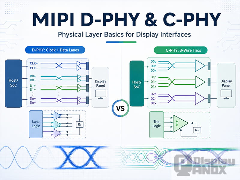
MIPI is one of the most common interface families used in modern display and camera systems. In display projects, it often appears in datasheets as MIPI DSI, MIPI DSI-2, MIPI D-PHY, or MIPI C-PHY. These terms are closely related, but they do not mean exactly the same thing.
A simple way to understand MIPI is to divide it into layers. The display or camera protocol defines how image data and control information are organized. The physical layer defines how those signals are transmitted electrically between chips, display panels, image sensors, bridge ICs, or control boards.
For display selection, the most practical question is not only whether a panel supports MIPI. The key questions are: which MIPI protocol is used, which physical layer carries the signal, how many lanes or trios are required, and whether the host platform can provide enough bandwidth and correct timing.
This article explains the physical layer side of MIPI, with a focus on D-PHY and C-PHY, two physical layers widely used in display and camera applications.
1. MIPI Protocol Layers and Physical Layer Types
MIPI can be understood from three levels: the application layer, the protocol layer, and the physical layer. For display and camera systems, the protocol layer is usually represented by specifications such as MIPI DSI, MIPI DSI-2, or MIPI CSI-2. The physical layer is represented by specifications such as D-PHY, C-PHY, M-PHY, and A-PHY.
Among these physical layers, D-PHY and C-PHY are the most relevant for compact display and camera links. They are normally used for short-distance communication, such as chip-to-chip, board-to-board, or processor-to-display connections inside a device. M-PHY is more commonly associated with applications such as high-speed storage, while A-PHY is designed for longer-reach links, especially in automotive environments.
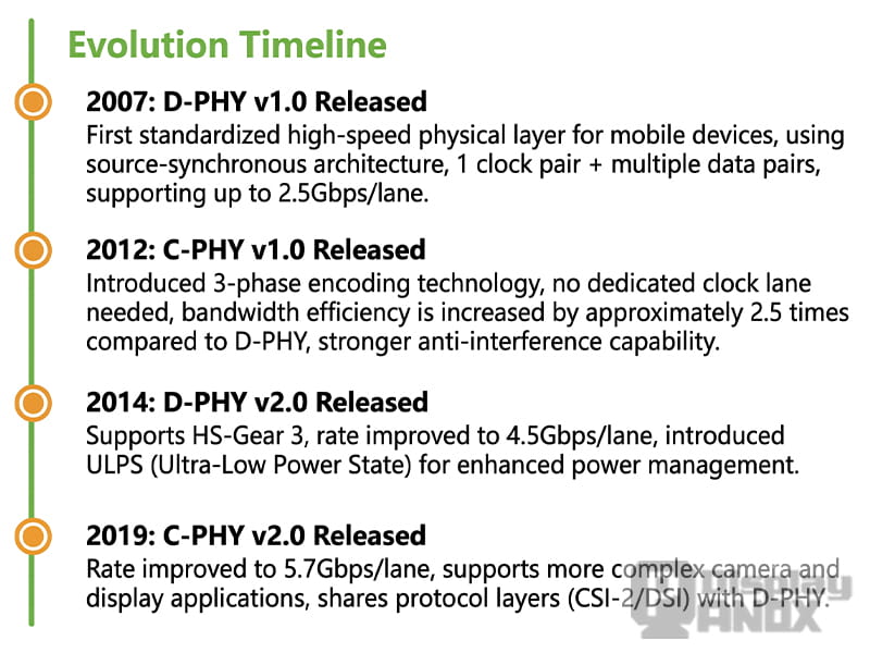
2. MIPI D-PHY and C-PHY Supported Data Rates
D-PHY and C-PHY have evolved to support higher camera resolutions, higher display refresh rates, and more demanding embedded vision applications.
D-PHY uses lanes. Its data rate is usually described as bits per second per lane. A common D-PHY display connection may use one, two, or four data lanes, plus one clock lane.
| No. | D-PHY Version | Encoding | Maximum Data Rate per Lane | Typical 4-Lane Total Bandwidth | Main Positioning |
|---|---|---|---|---|---|
| 1 | V1.2 | NRZ | 1.5 Gbps | 6 Gbps | Classic version widely used in earlier FHD smartphone cameras and displays |
| 2 | V2.5 | NRZ | 2.5 Gbps | 10 Gbps | Common mainstream choice with a balance of performance and cost |
| 3 | V3.0 | NRZ | 4.5 Gbps | 18 Gbps | Designed for 4K+, high refresh rate displays, and high-resolution sensors |
| 4 | V3.0 | PAM-4 | 9.0 Gbps | 36 Gbps | Higher-performance direction for future ultra-high-definition applications |
Table 1. Key performance comparison of different D-PHY versions
C-PHY uses trios instead of traditional two-wire differential lanes. Its data rate is usually described as symbols per second per trio. Because C-PHY encoding can carry about 2.28 bits per symbol in the commonly discussed 6-wirestate mode, it can provide high bandwidth with fewer signal wires.
| No. | C-PHY Version | Maximum Symbol Rate | Maximum Data Rate per Trio | Typical 3-Trio Total Bandwidth | Main Positioning |
|---|---|---|---|---|---|
| 1 | V1.0 | 2.5 Gsps | 5.7 Gbps | 17.1 Gbps | Early version that established the basis of C-PHY |
| 2 | V2.0 / V2.1 | 5.0 Gsps | 11.4 Gbps | 34.2 Gbps | High-performance version used in many advanced devices |
| 3 | V3.0 | Target ≥8.0 Gsps | ≥18.24 Gbps | ≥54.7 Gbps | Next-generation specification direction for higher bandwidth applications |
Table 2. Key performance comparison of different C-PHY versions
3. How MIPI Is Integrated in Chips and Display Modules
In real systems, MIPI can be integrated in two common ways.
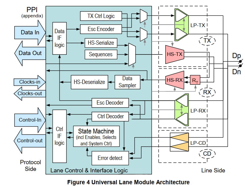
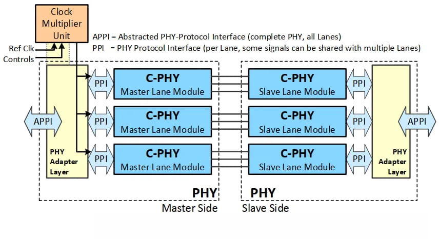
The first is a separated architecture. In some FPGA or ASIC designs, the CSI-2 or DSI-2 protocol controller IP and the D-PHY or C-PHY physical layer IP are separate blocks. They are connected internally through a PHY-Protocol Interface, often called PPI. In this architecture, the protocol controller prepares the outgoing data stream, while the physical layer processes and transmits the signal through the actual pins.
The second is an integrated architecture. This is more common from the perspective of display module users. Many chip vendors package the protocol layer and the physical layer together, then expose a complete MIPI CSI or MIPI DSI interface. For example, a display datasheet may simply write “MIPI DSI 4-lane,” while a camera datasheet may write “MIPI CSI-2 interface with 2-lane D-PHY.” This means the module already includes the necessary protocol and physical-layer support internally.
For display projects, the integrated description is often enough at the early selection stage. During debugging, however, engineers still need to confirm the lane count, physical layer type, clock setting, power sequence, initialization commands, and signal integrity conditions.
4. What the MIPI Physical Layer Does
The physical layer defines how digital data is converted into electrical signals and transmitted over wires. It covers transmission media, electrical characteristics, signal levels, clocking methods, timing rules, and state transitions.
For display interfaces, the physical layer is especially important because high-resolution images require large amounts of data to be delivered in a compact FPC connection. A mismatch in lane count, clock rate, signal quality, or timing can prevent a display from lighting up correctly even when the connector appears to fit.
5. MIPI D-PHY Architecture
D-PHY is one of the most widely used MIPI physical layers for cameras and displays. It uses a source-synchronous architecture with a dedicated differential clock lane and one or more differential data lanes.
A typical D-PHY interface can be configured as one, two, or four data lanes. The full common configuration contains four data lanes and one clock lane. The minimum practical configuration usually contains one data lane and one clock lane.
For example, when a display is described as a 4-lane MIPI DSI display, it usually means the interface has four data lane pairs plus one clock lane pair. When it is described as a 1-lane MIPI DSI display, it usually means one data lane pair plus one clock lane pair.
D-PHY data rate is described in bits per second per lane. For example, if each data lane runs at 1 Gbps, a four-lane D-PHY link has a theoretical lane-level data rate of 4 Gbps before protocol overhead and timing margins are considered.
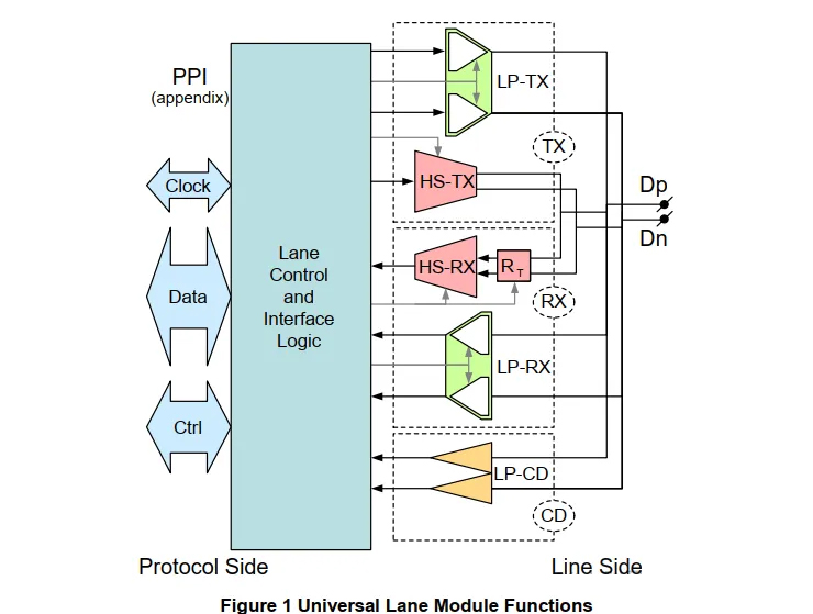
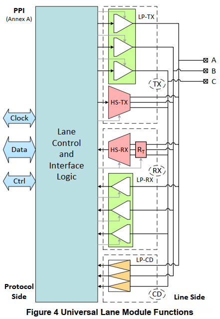
A general D-PHY lane module may include a high-speed receiver, high-speed transmitter, low-power receiver, low-power transmitter, low-power contention detector, and bias circuits. In actual products, the lane circuit may be simplified depending on whether the device mainly transmits or receives data.
6. D-PHY Working Modes: High-Speed, Low-Power, and Escape
D-PHY mainly works in two modes: High-Speed mode and Low-Power mode. It also supports Escape mode, which is a special operation under low-power conditions.
High-Speed mode, often written as HS mode, is used for large data transmission. In display applications, this usually means image data, video frames, or high-speed display packets. HS mode uses low-voltage differential signaling. It provides high data throughput, but it requires the high-speed circuit to be active.
Low-Power mode, often written as LP mode, is used for low-speed control communication. In display systems, LP mode is commonly used for initialization commands, register settings, sleep control, reset-related operations, or other command transmission. LP mode uses single-ended signaling with a higher voltage swing and lower data rate than HS mode.
Escape mode is used for special low-power operations, such as low-speed asynchronous data, trigger functions, or deeper low-power states.
This combination is one reason MIPI is suitable for compact display systems. The interface can transmit a large amount of image data in HS mode, then reduce activity and power consumption when only control communication is needed.
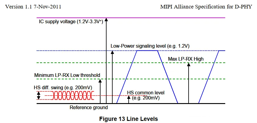
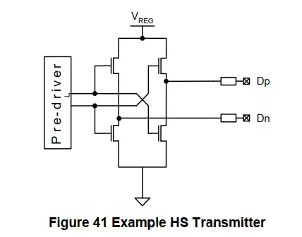
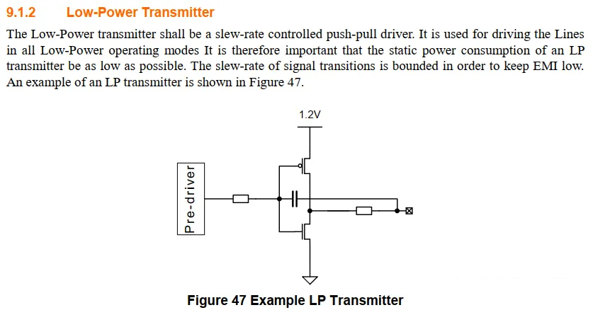
7. D-PHY Lane States
In HS mode, the D-PHY lane uses differential signaling, so each lane has two high-speed states.
| HS State | Dp Signal | Dn Signal |
|---|---|---|
| HS-0 | Low | High |
| HS-1 | High | Low |
In LP mode, the two wires in the lane are driven independently. This creates four possible low-power states.
| LP State | Dp Signal | Dn Signal |
|---|---|---|
| LP-00 | Low | Low |
| LP-01 | Low | High |
| LP-10 | High | Low |
| LP-11 | High | High |
LP-11 is commonly used as the Stop state. High-speed data transmission usually starts from the Stop state and returns to the Stop state after the burst is complete.
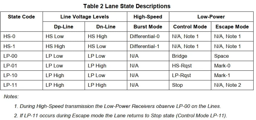
8. D-PHY High-Speed Burst Transmission
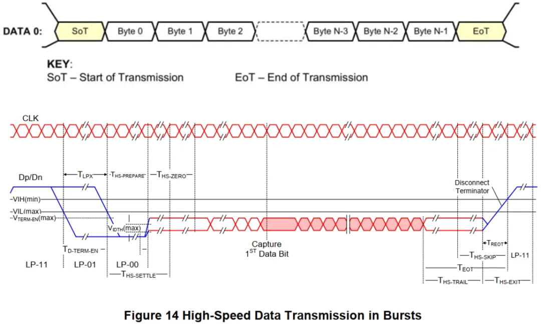
D-PHY high-speed transmission is usually organized as a burst. Before the payload data is transmitted, the transmitter and receiver need to enter the correct high-speed state and complete the required synchronization process.
A simplified high-speed transmission process is as follows:
The data lane starts from the Stop state, usually LP-11. When high-speed transmission is requested, the lane enters the high-speed transition sequence. The transmitter then sends the Start-of-Transmission sequence, followed by the actual payload data. After the payload is complete, the transmitter sends the End-of-Transmission sequence and returns the lane to the Stop state.
The clock lane also works in high-speed mode during high-speed data transfer. It provides a DDR clock, which means data is sampled on both clock edges. This improves bandwidth efficiency without simply increasing the clock frequency.
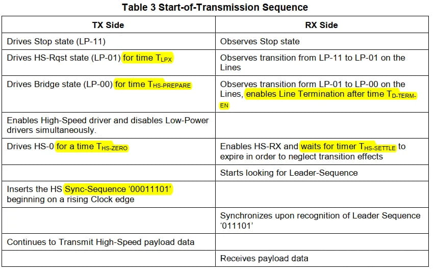
The Start-of-Transmission sequence helps the receiver detect that high-speed data transmission is beginning. In the original sequence, the lane enters high-speed mode through a state change such as LP-11 to LP-01 to LP-00, then begins the high-speed signaling process and synchronization sequence.
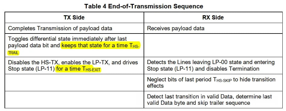
At the end of the burst, the transmitter completes the high-speed payload, sends the required end sequence, and returns the lane to LP-11. This makes the transmission boundary clear to the receiver and prepares the link for the next transmission.
For display debugging, this process matters because a black screen or unstable image may come from more than one cause. The issue may be related to the DSI command table, the display timing, the MIPI clock, the selected lane count, the power sequence, or signal quality on the FPC.
9. MIPI C-PHY Architecture
C-PHY is different from D-PHY in both wiring and encoding. Instead of using a traditional two-wire differential data lane and a separate clock lane, C-PHY uses a three-wire structure called a trio.
Each C-PHY trio contains three signal wires, usually described as A, B, and C. The receiver does not simply compare one positive and one negative wire. Instead, it evaluates the relationships between the three wires. The three wires are driven to different states, and the receiver determines the transmitted information by comparing the wire levels and detecting state transitions.
C-PHY does not transmit a separate clock signal. Clock information is embedded into the signal transitions and recovered by the receiver through clock and data recovery. This is one of the major differences between C-PHY and traditional D-PHY operation.
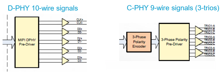
A C-PHY interface can use multiple trios. A three-trio C-PHY interface uses nine wires. By comparison, a common four-data-lane D-PHY interface with one clock lane uses ten wires. This makes C-PHY attractive in systems where high bandwidth, pin count, and electromagnetic behavior need to be balanced.
10. C-PHY Encoding and Data Efficiency
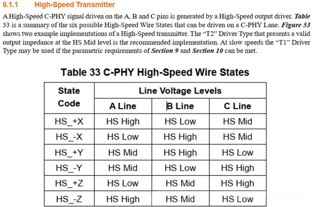
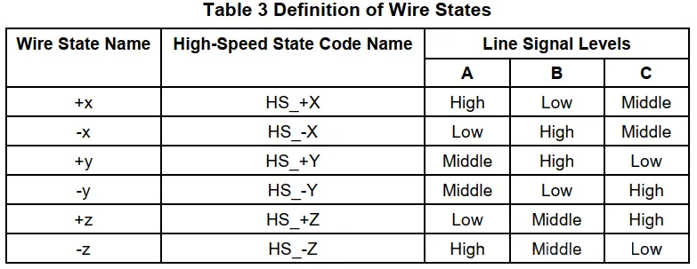
C-PHY uses three-phase symbol encoding. At any moment, the three wires in a trio are in different states. The protocol uses six possible wire states, commonly described as +x, -x, +y, -y, +z, and -z.
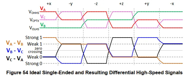
The physical link transmits different voltage levels on the A, B, and C wires. By calculating A-B, B-C, and C-A, the receiver can recover the wire state. Then, by observing the transition direction, phase, and polarity between states, the receiver recovers the encoded symbol and finally decodes the original data.
D-PHY data rate is typically described as bits per second per lane. C-PHY data rate is described as symbols per second per trio. In the commonly discussed 6-wirestate mode, seven symbols can encode 16 bits of data, giving an encoding factor of about 2.28 bits per symbol. This is why C-PHY can deliver high data throughput through a compact three-wire trio structure.
11. C-PHY HS and LP Modes
Like D-PHY, C-PHY also supports HS mode and LP mode. LP mode is used for low-power communication and control-related operations. HS mode is used for high-speed data transmission.
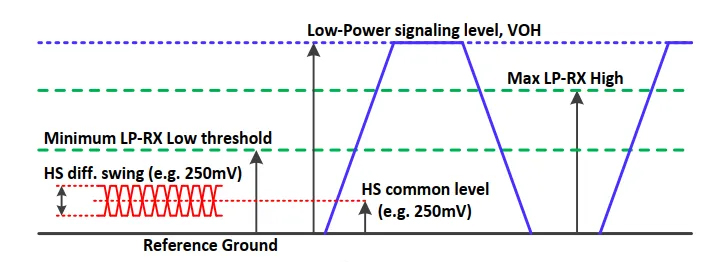
In LP mode, the signal level is similar to D-PHY low-power signaling, with a higher voltage swing. In HS mode, C-PHY operates around a lower common-mode level and uses multiple signal levels to represent different wire states.
The following state table shows how C-PHY high-speed wire states are represented by the A, B, and C line levels. These states form the basis for C-PHY transition encoding.
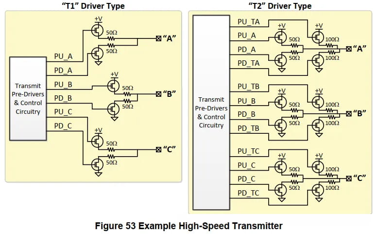
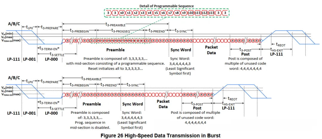
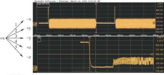
12. C-PHY Waveform and Eye Diagram
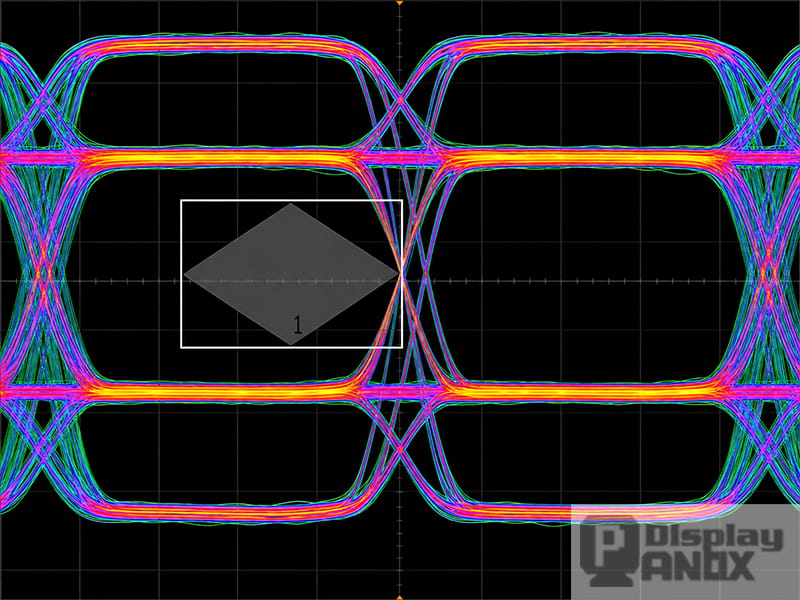
C-PHY waveforms look different from traditional two-wire differential signaling. In HS mode, the A, B, and C wires in one trio may appear as high, middle, and low voltage levels when measured relative to ground. When the receiver calculates the differences between wire pairs, the result creates multiple differential levels.
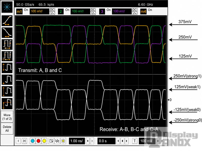
This multi-level behavior also changes the eye diagram. A D-PHY differential signal usually has a more familiar two-level eye pattern. C-PHY has multiple differential levels, so its eye diagram contains more openings and requires a different interpretation method.
13. C-PHY Strong and Weak States
Inside one C-PHY trio, the three wires A, B, and C can be compared in pairs: VA-VB, VB-VC, and VC-VA. These comparisons create different differential levels. From high to low, they can be described as strong 1, weak 1, weak 0, and strong 0.
For example, in one wire state, VA-VB may produce the strongest positive differential result, which is defined as strong 1. In another state, the same comparison may produce a weaker positive result, defined as weak 1. The same method can be used to identify weak 0 and strong 0.
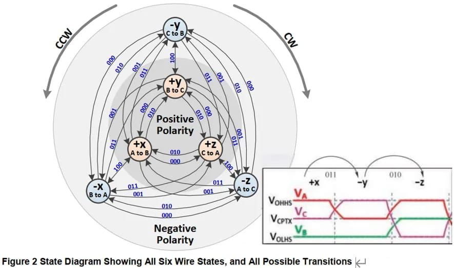
Because C-PHY encodes both data and clock information into transitions, even repeated data patterns still require signal transitions. This allows the receiver to recover timing without a separate clock lane.
For example, when the line state changes from +x to -y, the transition can represent one symbol. When it changes from -y to -z, it can represent another symbol. If the same symbol needs to continue, the line state still changes to another valid state instead of remaining static. This is a key reason C-PHY does not need an additional forwarded clock lane in the same way as traditional D-PHY operation.
14. D-PHY vs C-PHY for Display Applications
D-PHY and C-PHY are both used to carry high-speed display and camera data, but they are designed with different trade-offs.
D-PHY is widely adopted, easy to understand from a lane-count perspective, and supported by many application processors, bridge ICs, display driver ICs, LCD panels, AMOLED panels, and Micro OLED modules. For many embedded display projects, D-PHY remains the most familiar and practical MIPI physical layer.
C-PHY is more efficient in terms of data carried per wire group. It uses three-wire trios and embedded clocking, which can reduce the need for a separate clock lane and improve bandwidth efficiency. However, C-PHY requires support from both the host and the display side. A D-PHY-only host cannot directly drive a C-PHY-only display without a compatible bridge or dual-mode interface.
| Comparison Item | D-PHY | C-PHY |
|---|---|---|
| Basic unit | Lane | Trio |
| Wire structure | Differential pair | Three-wire trio |
| Clocking method | Dedicated clock lane in traditional operation | Embedded clock |
| Common rate unit | Gbps per lane | Gsps per trio |
| Data efficiency | Straightforward lane-based transmission | About 2.28 bits per symbol in common 6-wirestate mode |
| Main advantage | Mature ecosystem and broad compatibility | Higher wire efficiency and no separate clock lane |
| Typical display use | LCD, AMOLED, Micro OLED, embedded display modules | Advanced high-bandwidth display and camera systems |
15. How to Read a MIPI Display Panel Datasheet
When selecting a MIPI display module, the interface name alone is not enough. A display described as “MIPI DSI” may still require many additional details before it can be matched with a host board.
The following items should be checked carefully:
| Datasheet Item | Why It Matters |
|---|---|
| MIPI protocol | Confirms whether the panel uses DSI, DSI-2, CSI-2, or another protocol |
| Physical layer | Confirms whether the panel uses D-PHY, C-PHY, or a dual-mode PHY |
| Lane or trio count | Determines host compatibility and available bandwidth |
| Resolution | Affects required pixel data rate |
| Refresh rate | Higher refresh rates require higher link bandwidth |
| Color depth | RGB565, RGB666, RGB888, or higher formats change bandwidth requirements |
| Video mode or command mode | Affects transmission behavior and initialization |
| MIPI clock range | Must match the host output capability |
| Initialization commands | Required to start the display driver IC correctly |
| Power sequence | Incorrect power timing may prevent the display from working |
| FPC pin definition | Determines mechanical and electrical compatibility |
For example, a 5.5 inch AMOLED display with 1080 × 1920 resolution and 4-lane MIPI DSI cannot be selected only by resolution and connector shape. The host must support the correct lane count, DSI mode, MIPI clock, power sequence, reset timing, and initialization code.
16. Why the MIPI Physical Layer Matters in Display Projects
The physical layer is often invisible to end users, but it directly affects whether a display solution works reliably. A display module may fail because of an incorrect software command sequence, but it may also fail because the physical link has insufficient margin.
Common MIPI-related issues include black screen, unstable image, flicker, random lines, abnormal color, failure at high refresh rate, or display behavior that changes when the FPC is moved. These problems may be caused by bandwidth mismatch, lane configuration errors, poor impedance control, skew between lanes, connector issues, insufficient grounding, or incorrect signal levels.
For display suppliers and product developers, this is why MIPI interface confirmation should happen early. A reliable display solution should consider the panel, driver IC, host processor, FPC, connector, timing parameters, command sequence, and power design together.
Panox Display supports display projects that use MIPI DSI, D-PHY, and related embedded display interfaces across LCD, AMOLED, Micro OLED, round display, long strip display, and custom display module applications. For customers choosing a MIPI display panel, the goal is not only to find a panel with the right size and resolution, but also to make sure the interface can be integrated into the target device with practical engineering support.
17. Conclusion
MIPI D-PHY and C-PHY are two important physical layers for modern display and camera systems. D-PHY uses a lane-based structure with a dedicated clock lane in traditional operation, making it mature, widely supported, and practical for many embedded display modules. C-PHY uses three-wire trios, embedded clocking, and more efficient symbol encoding, making it suitable for high-bandwidth applications where wire count and signal efficiency matter.
For display selection, the most important point is compatibility. A MIPI display module should be evaluated by protocol type, physical layer, lane or trio count, bandwidth, timing, initialization commands, power sequence, and host support. When these factors are matched correctly, MIPI provides a compact, high-speed, and power-efficient interface for modern display solutions.
Learn more: How to Bring Up a MIPI DSI Display: A Practical Guide for Embedded Display Integration
FAQ
What is MIPI D-PHY?
MIPI D-PHY is a physical layer used for high-speed data transmission in camera and display systems. In display products, it is commonly used together with MIPI DSI or MIPI DSI-2.
What is MIPI C-PHY?
MIPI C-PHY is a physical layer that uses three-wire trios and embedded clock encoding. It can provide high bandwidth with fewer signal wires compared with traditional lane-based approaches.
What is the difference between MIPI DSI and MIPI D-PHY?
MIPI DSI is a display protocol. MIPI D-PHY is a physical layer that carries the DSI signal electrically. A display may use MIPI DSI over D-PHY.
What does 4-lane MIPI DSI mean?
A 4-lane MIPI DSI display usually uses four D-PHY data lanes plus one clock lane. It is common in higher-resolution LCD, AMOLED, and Micro OLED display modules.
Can a D-PHY host drive a C-PHY display?
In most cases, no. A D-PHY-only host cannot directly drive a C-PHY-only display. The host and display must support the same physical layer, or a compatible bridge solution is required.