







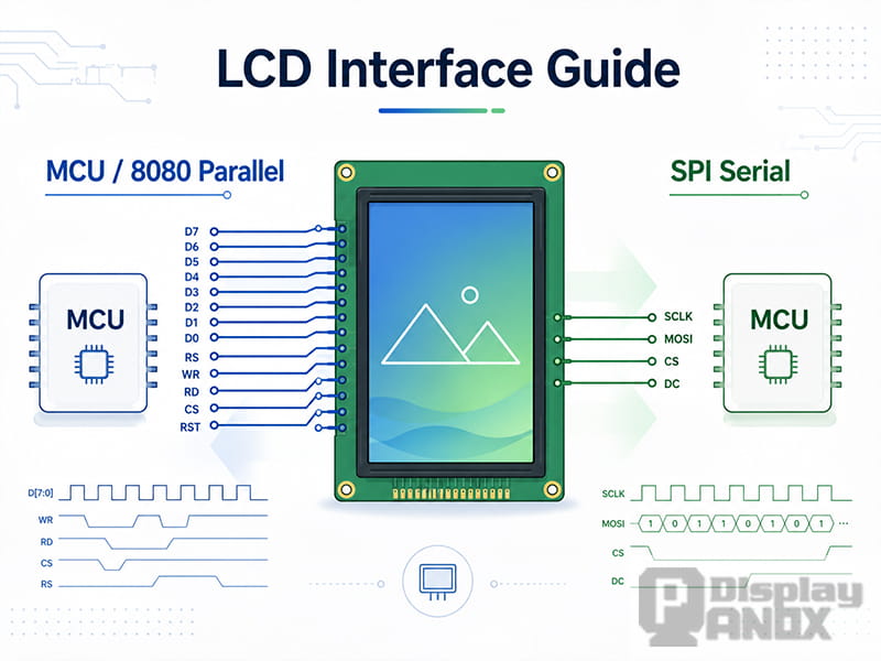
LCD modules can use many different interface types depending on screen size, resolution, refresh requirements, controller IC, product structure, and system cost. For embedded display projects, two of the most common physical interfaces are the MCU interface, often known as the 8080 parallel interface, and the SPI interface, a serial interface widely used on small TFT LCD modules.
Both interfaces are commonly found in compact display modules with built-in driver ICs and display memory. They are often used in handheld devices, industrial controllers, wearable devices, smart home panels, medical equipment, testing tools, and other embedded systems where a host MCU needs to send commands and pixel data directly to the LCD.
This guide explains how MCU 8080 and SPI LCD interfaces work, what their signal pins mean, how write and read cycles are handled, and how to choose between them in real display projects.
1. What Is an LCD Display Interface?
An LCD display interface is the electrical and communication link between the host processor and the display module. It defines how commands, parameters, and display data are transferred from the main controller to the LCD driver IC.
In a complete display product, the interface affects several key design factors:
-
Required MCU or processor pins
-
PCB routing complexity
-
Data bandwidth
-
Refresh performance
-
Driver development difficulty
-
Power consumption
-
Module cost
-
Suitable display size and resolution
Common LCD interfaces include MCU/8080, SPI, RGB, LVDS, MIPI DSI, eDP, HDMI, and other application-specific solutions. Among them, MCU and SPI are especially common in small and medium embedded LCD modules because they are relatively simple to control and do not always require a high-performance application processor.
MIPI DBI, or Display Bus Interface, also describes several host-to-display controller bus types. In this classification, the Intel 8080-style parallel bus is generally associated with DBI Type B, while SPI-style serial communication is associated with DBI Type C.
2. MCU Interface: 8080 Parallel LCD Interface
The MCU interface is a parallel display interface used between a microcontroller and an LCD driver IC. In many datasheets and module specifications, it is also called the 8080 interface, Intel 8080 interface, parallel MCU interface, or DBI parallel interface.
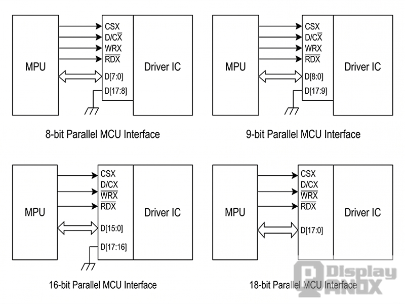
The 8080 LCD interface transfers data through multiple parallel data lines. Common bus widths include 8-bit, 9-bit, 16-bit, and 18-bit. A wider bus can transfer more data per cycle, but it also requires more MCU pins and more PCB traces.
The main advantage of the MCU interface is that it is straightforward to control. It does not require a continuous pixel clock, HSYNC, VSYNC, or DE signal like an RGB interface. The host sends commands and display data to the LCD driver IC, and the driver IC stores image data in its internal display RAM, often called GRAM.
The trade-off is that the display controller and its internal memory become important. For larger screens or high-frame-rate image updates, the interface bandwidth and GRAM-based update method may become limiting factors. For this reason, MCU interfaces are usually more suitable for small and medium LCD modules rather than high-resolution video displays.
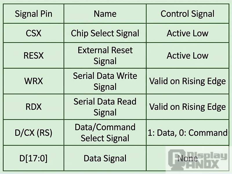
2.1 Common MCU 8080 Interface Signals
A typical 8080 MCU interface includes a chip select signal, command/data selection signal, write signal, read signal, reset signal, and parallel data bus.
| Signal | Common Name | Function |
|---|---|---|
| CSX / CS | Chip Select | Enables the LCD interface, usually active low |
| D/CX / RS / A0 | Data/Command Select | Selects whether the bus carries command or data |
| WRX / WR | Write Enable | Controls write timing from host to LCD |
| RDX / RD | Read Enable | Controls read timing from LCD to host |
| RESX / RESET | Reset | Resets the LCD driver IC |
| D[7:0] / D[15:0] / D[17:0] | Data Bus | Transfers command, parameter, or display data |
In controller IC documentation, D/CX is commonly used to distinguish command and data. When D/CX is low, the transferred value is interpreted as a command. When D/CX is high, the value is interpreted as a command parameter or display data. The ILI9341 datasheet describes this same command/data selection behavior, while WRX and RDX serve as write and read control signals in 8080-type MCU systems.
2.2 Different Parallel Bus Widths
The 8080 MCU interface can be configured with different data bus widths depending on the display driver IC and the host MCU design.
An 8-bit parallel interface uses fewer pins and is easier to route, but it needs more transfer cycles to send the same amount of pixel data. A 16-bit or 18-bit parallel interface can move more display data per write cycle and is more suitable for faster screen updates, but it consumes more GPIO resources and increases routing complexity.
For compact embedded products, 8-bit MCU interfaces are still widely used. For products that require smoother UI updates or higher color depth, 16-bit or 18-bit MCU interfaces may be selected when the host controller has enough available pins.
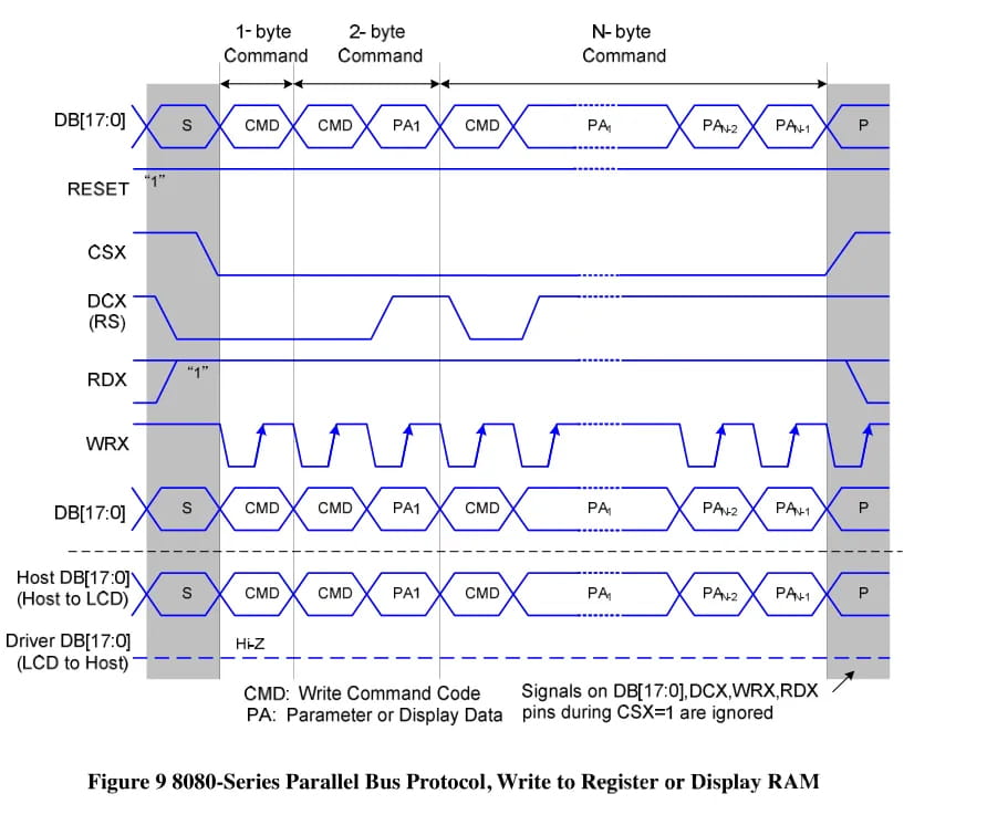
2.3 MCU 8080 Write Cycle
The write cycle is used when the host writes a command, parameter, or display data to the LCD driver IC.
In a typical 8080 write operation, the host first pulls CSX low to select the display. The D/CX signal is then set according to the type of information being sent. If D/CX is low, the value on the data bus is treated as a command. If D/CX is high, the value is treated as display data or a command parameter.
During the write cycle, WRX changes state to indicate that valid data is present on the bus. The LCD driver samples the data bus according to the WRX timing. In ST7789V documentation, the 8080 write cycle is described as a WRX high-low-high sequence involving control signals such as DCX, RDX, and WRX, along with the parallel data bus.
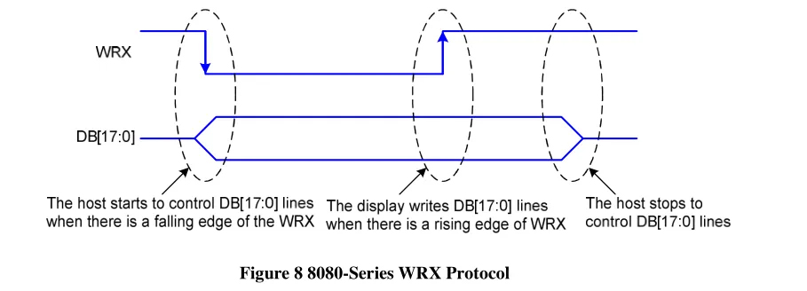
The write sequence can be used to send register commands, display configuration parameters, gamma settings, address window settings, or pixel data to the display RAM.
2.4 MCU 8080 Read Cycle
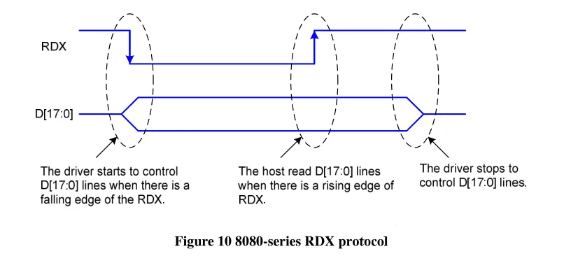
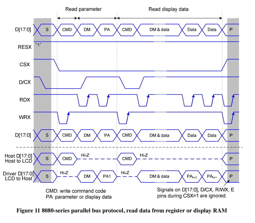
The read cycle is used when the host needs to read data back from the LCD driver IC. Typical read operations include reading display status, ID information, register values, or display RAM data if the controller supports it.
For a read operation, the host selects the display by pulling CSX low, sets the required command, and then controls RDX to read data back from the LCD. The data direction changes from host-to-display to display-to-host, so the host side must be able to release or switch the data bus correctly.
The timing requirements can vary between display controller ICs. Some controllers require a dummy read cycle before valid data is returned, which is also noted in NXP’s 8080 LCD interface application material.
Reading from display RAM or registers is less common in simple UI applications, but it can be useful during initialization verification, debugging, or status detection.
3. SPI Interface for LCD Modules
SPI, or Serial Peripheral Interface, is a serial communication interface widely used in embedded electronics. Compared with the MCU 8080 interface, SPI uses far fewer signal lines, which makes it attractive for compact devices, low-pin-count MCUs, and small display modules.
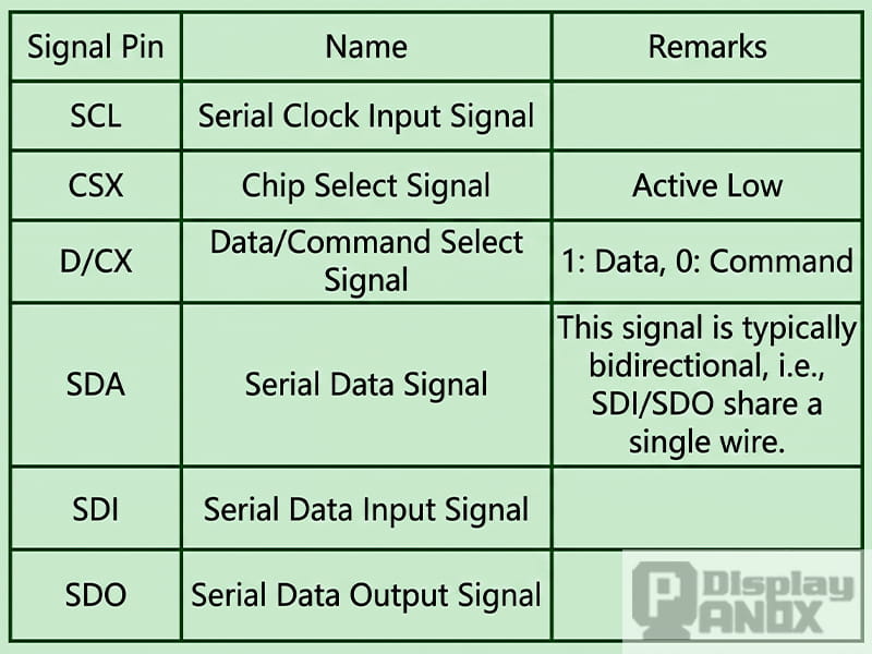
An SPI LCD interface usually includes signals such as CS, SCL/SCK, SDA/MOSI, optional SDO/MISO, DC/RS, and RESET. Espressif’s SPI LCD documentation also describes common SPI LCD pin naming such as CS, SCK/SCL, SDA/MOSI, SDO/MISO, and DC/RS.
The main advantage of SPI is simple wiring. The limitation is bandwidth. Since data is transferred serially, SPI usually cannot refresh large or high-resolution displays as quickly as a parallel MCU interface, RGB interface, or MIPI DSI interface. For this reason, SPI is most commonly used on small TFT LCDs, round displays, wearable screens, status panels, instrument displays, and control modules where the UI does not require full-screen high-frame-rate animation.
3.1 Common SPI LCD Interface Modes
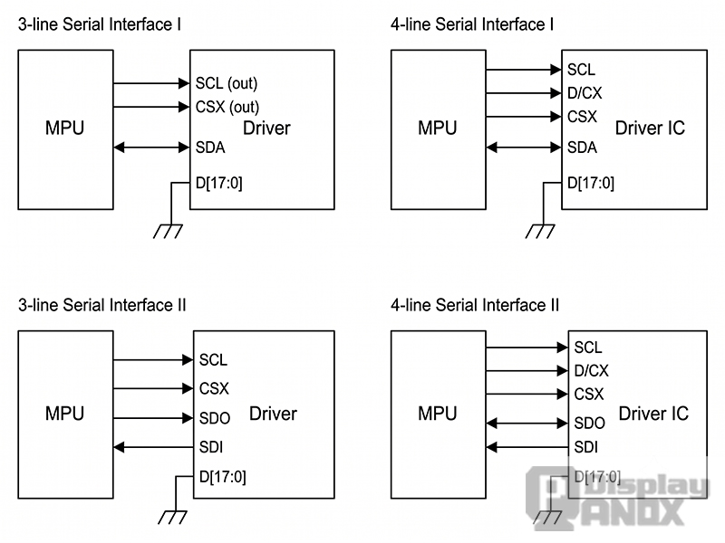
SPI LCD modules are often described as 3-wire or 4-wire interfaces. Some display controller ICs further divide these into Serial Interface I and Serial Interface II.
Common modes include:
| Mode | Description | Typical Signal Logic |
|---|---|---|
| 3-wire 9-bit SPI | Uses one serial data line, with a data/command bit included in the serial packet | Fewer pins, command/data carried in the data stream |
| 4-wire 8-bit SPI | Uses a separate D/C pin to distinguish command and data | More common and easier for many MCU platforms |
| Serial Interface I | Often uses the same serial data line for write and read behavior depending on controller design | Pin-efficient |
| Serial Interface II | May use separated input/output behavior depending on controller IC | Better readback support in some systems |
The ST7789V datasheet lists 3-line serial interface I, 4-line serial interface I, 3-line serial interface II, and 4-line serial interface II as selectable serial interface modes. It also describes 3-line serial communication using CSX, SCL, and SDA, while 4-line serial communication adds D/CX as a separate data/command signal.
3.2 Different SPI Connection Types
A 3-wire SPI LCD interface normally reduces pin count by embedding the command/data selection bit into the serial transfer. This makes the wiring compact, but it may not be supported directly by every MCU hardware SPI peripheral without special configuration.
A 4-wire SPI LCD interface uses a separate D/C signal. This is often easier to implement because commands and data are still transferred as standard 8-bit values, while the D/C pin tells the LCD whether the incoming byte is a command or display data.
In practical embedded designs, 4-wire SPI is often preferred when the MCU has enough pins, because it is easier to drive with common SPI hardware and software libraries.
3.3 SPI Write Cycle
The SPI write mode is used when the host sends commands or display data to the LCD.
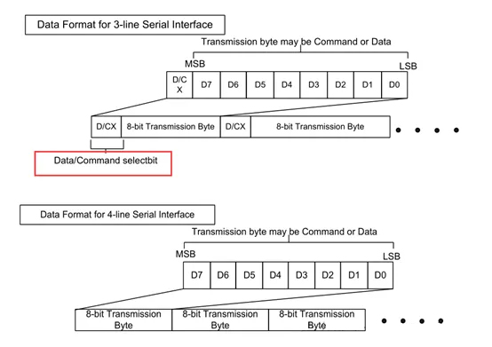
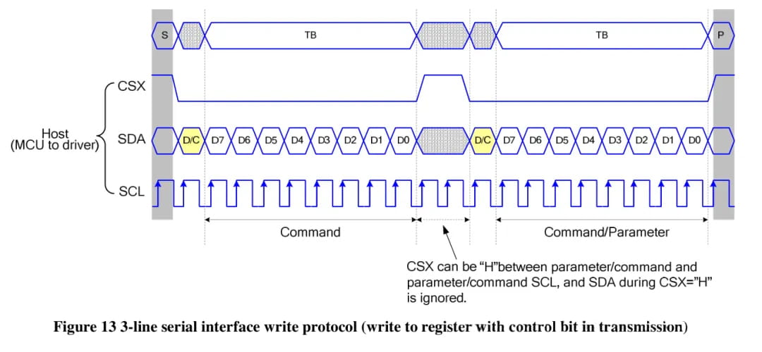
In a 3-wire 9-bit serial format, each transferred unit includes one D/CX selection bit and an 8-bit command or data byte. If the D/CX bit is low, the following byte is treated as a command. If the D/CX bit is high, the following byte is treated as display data or a command parameter.
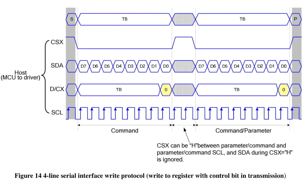
In a 4-wire 8-bit SPI format, the D/C signal is placed on a separate pin. The host sets D/C low for commands and high for data, while the actual command or data byte is transferred over SDA/MOSI according to the SCL/SCK clock.
During SPI writing, the host usually sends the most significant bit first. CS must be active during the transfer; when CS is inactive, the LCD ignores the serial input. After initialization commands are sent, pixel data can be written to the display RAM through address window commands and memory write commands.
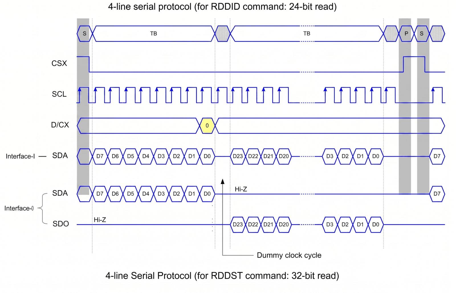
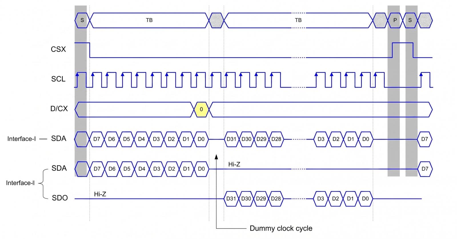
3.4 SPI Read Cycle
The SPI read mode is used when the host reads register values, display status, ID information, or other returned data from the LCD driver IC.
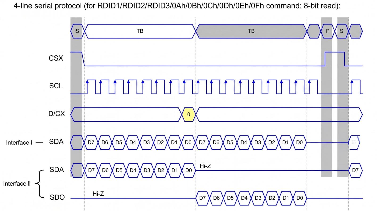
A typical SPI read operation starts with the host sending a read command. After the command phase, the bus direction changes so that the LCD can return data to the host. Depending on the controller IC and selected SPI mode, the returned data may use the same SDA line or a separate SDO/MISO line.
The host must pay attention to timing details. For example, the input data may be sampled on one clock edge while output data is shifted on the opposite edge. Some read commands also include dummy clocks or dummy bytes before valid returned data appears.
In 3-wire SPI read operation, the shared data line must be released by the host before the LCD starts driving output data. Otherwise, bus contention may occur.
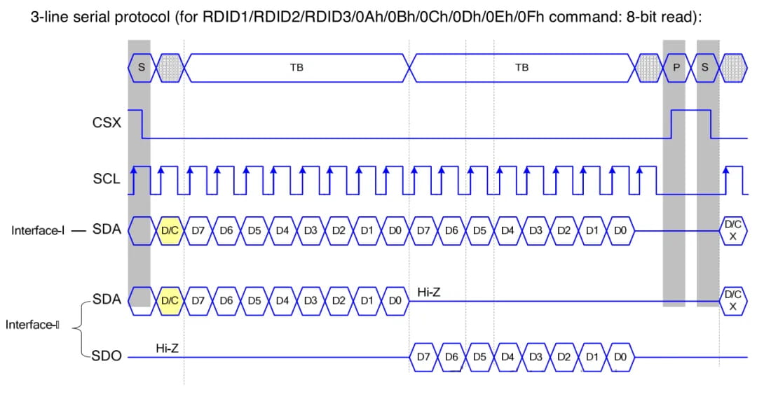
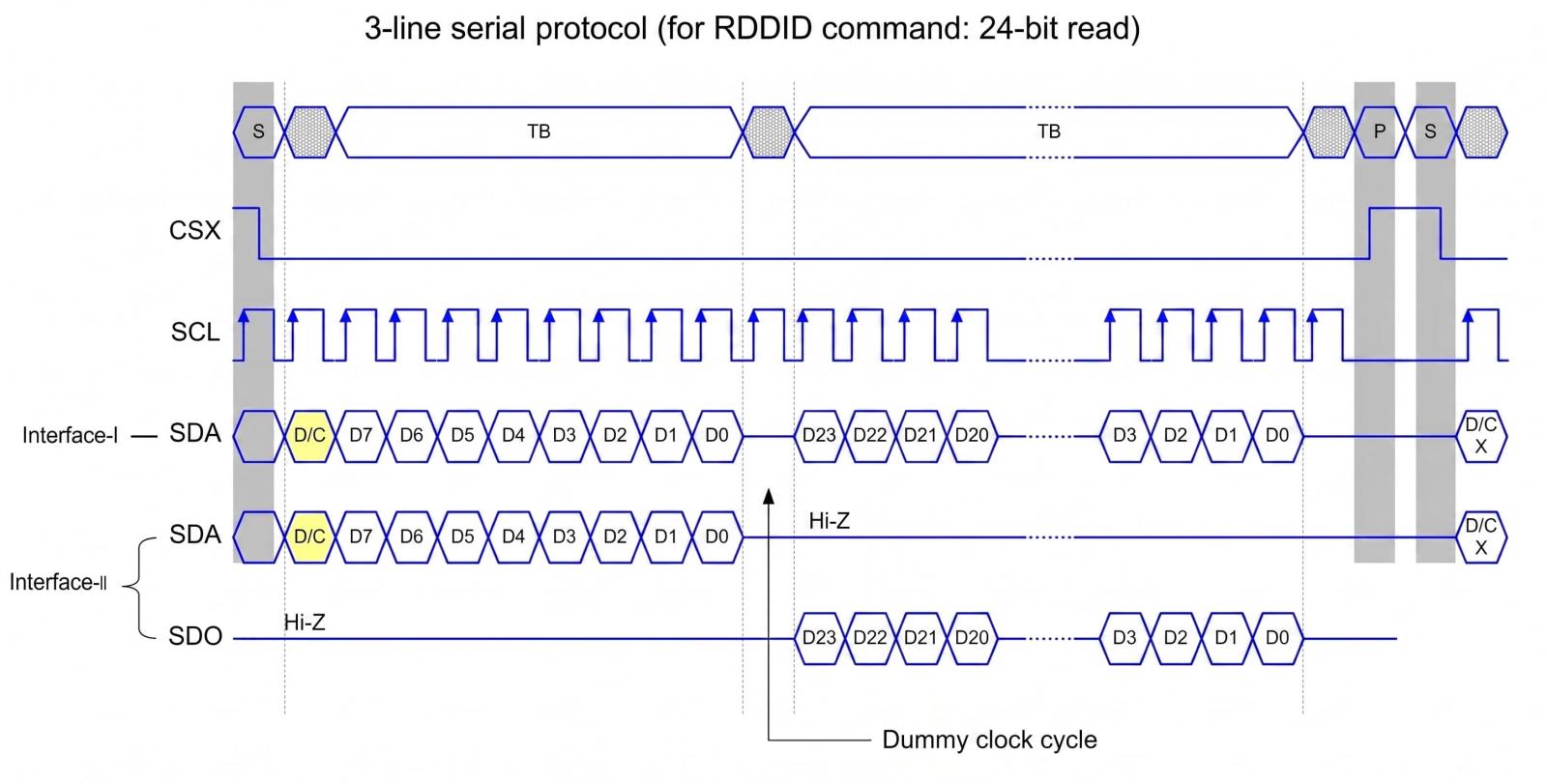
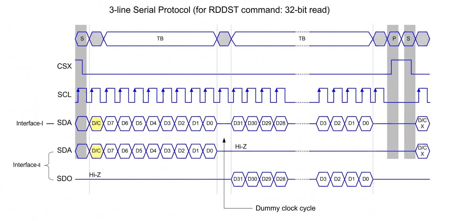
For 4-wire SPI read operation, the readback path may use a separate output line, which can make the bus direction easier to manage. However, actual support depends on the LCD driver IC, the module pinout, and whether the SDO/MISO pin is available on the FPC or module connector.
4. MCU 8080 vs SPI LCD Interface: Key Differences
Although MCU 8080 and SPI interfaces are both common in embedded LCD modules, they are suitable for different design priorities.
| Item | MCU 8080 Interface | SPI Interface |
|---|---|---|
| Data transfer | Parallel | Serial |
| Typical bus width | 8-bit, 9-bit, 16-bit, 18-bit | 3-wire 9-bit or 4-wire 8-bit |
| Pin count | Higher | Lower |
| PCB routing | More complex | Simpler |
| Bandwidth | Higher than SPI under similar conditions | Lower because data is sent serially |
| Control difficulty | Simple, but requires more GPIO | Simple wiring, software may vary by mode |
| Common use | Small to medium TFT LCDs, embedded GUI panels | Small TFT LCDs, round displays, status screens |
| Best for | Faster partial or full-screen updates with available pins | Low-pin-count compact designs |
For a small control panel, a wearable display, or a status screen, SPI may be the most practical choice. It reduces connector pins and simplifies layout, especially when the screen resolution is not too high.
For a display that needs faster screen updates, a richer graphical UI, or higher pixel throughput, an 8080 MCU parallel interface may be more suitable if the host MCU has enough pins.
For high-resolution video display, smartphone-class panels, AR/VR displays, or larger industrial screens, interfaces such as RGB, LVDS, MIPI DSI, or eDP are usually more appropriate than MCU or SPI.
5. How to Choose the Right LCD Interface for a Project
Interface selection should not be based only on the number of pins. A better approach is to evaluate the full display system, including screen size, resolution, refresh behavior, MCU capability, board space, and software resources.
For compact products with limited GPIO, SPI LCD modules are attractive because they need fewer signal lines and are easier to connect. They are suitable for simple UI, icons, text, sensor data, menu screens, and static or semi-static graphics.
For products that need faster image updates but still use an MCU-based architecture, 8080 parallel LCD modules can provide better throughput. This is useful for embedded GUIs, handheld instruments, industrial HMIs, and small control terminals.
For projects that require continuous video, high resolution, high refresh rate, or advanced graphics rendering, MCU and SPI interfaces may not be enough. In those cases, RGB, LVDS, MIPI DSI, HDMI, or eDP should be considered.
Panox Display supports display module selection based on interface type, display size, resolution, brightness, touch panel structure, FPC design, cover glass, and application environment. For embedded LCD projects, the interface should be confirmed early because it affects the main board design, connector definition, firmware development, and long-term product compatibility.
6. Conclusion
The MCU 8080 interface and SPI interface are two important LCD connection methods for embedded display systems.
The MCU 8080 interface uses a parallel data bus and is suitable for applications that need higher data throughput while still keeping the control method relatively simple. It requires more pins, but it can support faster display updates than SPI in many small and medium LCD applications.
The SPI interface uses fewer signal lines and is easy to route, making it ideal for compact devices and small LCD modules. Its bandwidth is more limited, so it is better suited for simple UI, status display, wearable screens, and low-to-medium refresh applications.
Choosing the right LCD interface depends on the balance between pin count, bandwidth, display size, resolution, refresh performance, and product structure. A clear understanding of MCU and SPI interface behavior helps engineers select a display module that matches both hardware design and user experience requirements.