







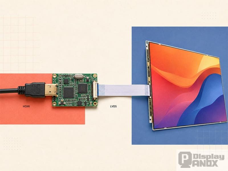
An HDMI to LVDS converter is an active display bridge or controller board that connects an HDMI video source to an LCD panel with an LVDS input. It receives the HDMI signal, completes the source-to-display handshake, recovers the video data and timing, and repackages that data into the LVDS format expected by the panel.
This conversion cannot be achieved with a passive cable. HDMI and panel-level LVDS differ in signaling, data organization, clocking, control functions and power requirements. A working solution therefore depends on much more than finding connectors with the same number of pins.
The typical signal path is:
HDMI source → HDMI receiver → optional scaler or video processor → LVDS serializer → LCD timing controller
The same board may also manage EDID, panel power, backlight brightness, audio extraction, on-screen display controls and touch connectivity.
What Does an HDMI to LVDS Converter Actually Convert?
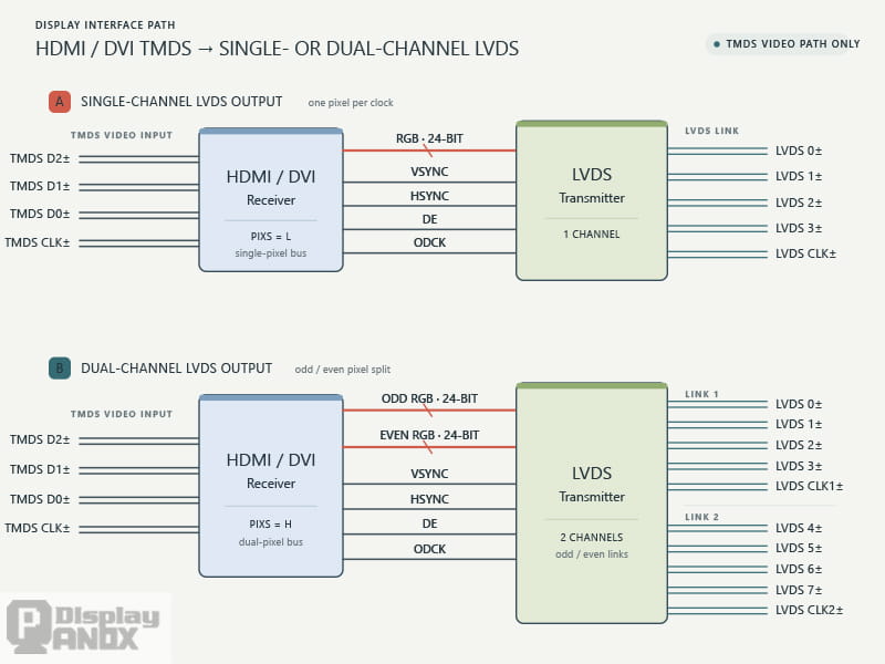
Single- and dual-channel HDMI-to-LVDS conversion paths
HDMI is a system-level interface used between devices such as computers, media players, cameras and displays. It carries digital video together with audio and control data. The HDMI Licensing Administrator describes HDMI as an interface serving consumer electronics, PCs, automotive systems, commercial AV equipment and industrial applications.
The LVDS connection inside an LCD system has a different purpose. It transports serialized RGB pixel data and timing signals from a controller to the panel timing controller. In display specifications, this interface may also be described as OpenLDI, FPD-Link or simply a panel LVDS interface.
In a typical TMDS-based HDMI implementation, the input arrives through three differential data pairs and one clock pair. A conventional LVDS panel interface uses three or four data pairs plus a clock pair for each channel. Higher-bandwidth panels may use two LVDS channels, producing six or eight data pairs and two clock pairs.
A Texas Instruments HDMI/DVI-to-LVDS application report illustrates this process with a receiver and an LVDS transmitter. The receiver reconstructs parallel RGB data, synchronization signals and the pixel clock. The transmitter then serializes that information for the LCD panel.
The board is therefore rebuilding and reorganizing the video stream rather than merely changing its voltage level.
How Does an HDMI to LVDS Converter Work?
1. HDMI connection detection and EDID exchange
When an HDMI source is connected, the converter board acts as the display device. Hot Plug Detect informs the source that a display is present, while the Display Data Channel allows the source to read the board’s EDID.
EDID describes the video modes accepted by the receiving system, including supported resolutions and timing information. Texas Instruments defines it as a data structure that lists display capabilities so that the video source can generate an appropriate resolution and timing.
In many converter boards, this information is stored in an EEPROM or internal memory. It does not necessarily come directly from the bare LCD panel. The EDID therefore has to match the converter firmware, scaler capability and panel timing. An incorrect EDID can cause the source to output an unsupported resolution even when the HDMI connection itself is detected correctly.
2. HDMI signal reception and decoding
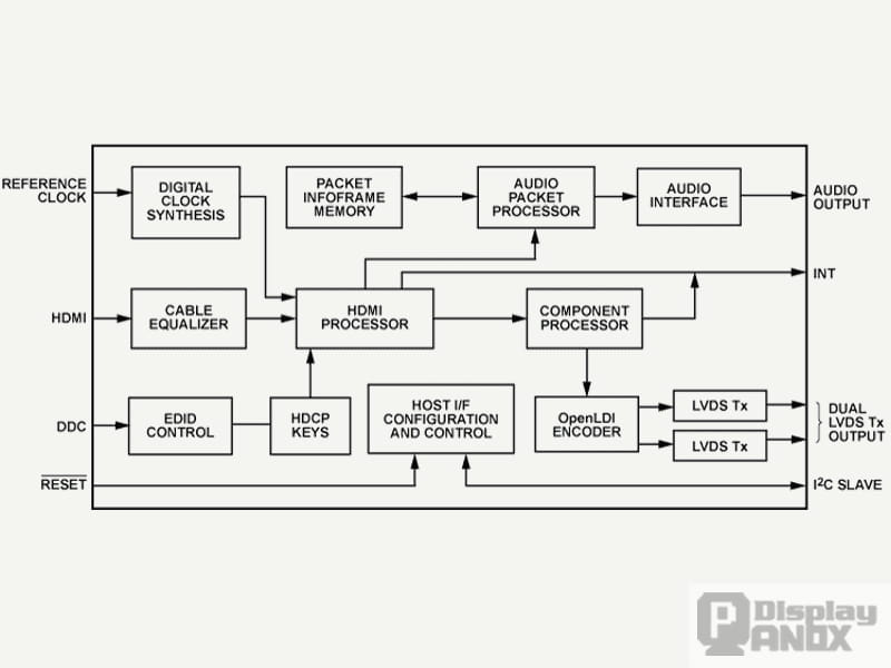
Functional blocks inside an HDMI-to-LVDS display bridge
The HDMI receiver equalizes the incoming signal, recovers the clock and decodes the video stream. Depending on the chipset, it may output RGB or YCbCr pixel data together with HSYNC, VSYNC, data enable and pixel clock signals.
Audio can also be extracted at this stage, but it follows a separate path. A conventional LVDS panel link carries display pixel and control data rather than HDMI audio. Boards with speakers, headphone outputs, I²S or S/PDIF connections must route the audio independently.
The Analog Devices ADV7613 provides a useful example of an integrated HDMI-to-LVDS display bridge. It combines an HDMI receiver, EDID memory, color-space processing and configurable LVDS output in one device. Its published architecture also shows why a complete converter involves substantially more circuitry than a connector adapter.
3. Scaling and timing generation
A direct HDMI-to-LVDS bridge normally converts the interface while preserving a compatible input timing. If the HDMI source cannot generate the panel’s required timing, a bridge alone may not produce a stable image.
An LCD controller board with a scaler has broader capabilities. It can receive standard HDMI resolutions, buffer or scale the image, and generate the panel’s native output timing. The controller may also handle aspect ratio, image position, color controls and an on-screen menu.
The presence of an HDMI input does not prove that a board contains a scaler. This distinction should be confirmed before selection.
4. RGB mapping and LVDS serialization
After timing has been prepared, the pixel data must be mapped into the lane order used by the panel. A common 24-bit implementation combines RGB888 data with synchronization and control bits, then serializes the parallel data across four LVDS data pairs.
Many LVDS transmitters use a 7:1 serialization ratio. Each data pair carries seven serialized bits during one pixel-clock period, while a separate differential pair carries the LVDS clock. The operating pixel-clock range depends on the transmitter rather than on LVDS as a general concept.
Dual-channel LVDS divides the pixel stream between two links, commonly as odd and even pixels. This reduces the clock frequency required by each link. For example, a conventional 1920 × 1080 at 60 Hz timing may use a 148.5 MHz full-rate pixel clock while a dual-pixel LVDS implementation operates each link at 74.25 MHz. The exact timing still has to follow the panel specification.
5. Panel power and backlight control
The LVDS cable is only part of the display system. The converter board may also have to supply the panel logic voltage, backlight power, backlight enable and PWM brightness control.
These functions require the correct voltage, current capacity, polarity and startup sequence. A typical sequence applies panel power, establishes stable LVDS video and then enables the backlight. The shutdown sequence generally reverses that order. The TI DS90C185 documentation provides an example in which valid black video is established before the backlight is enabled.
A board can therefore produce a working backlight while the pixel interface remains incorrectly configured. Backlight operation alone does not confirm LVDS compatibility.
HDMI-to-LVDS Bridge, Scaler Board or FPGA?
Several architectures can perform HDMI-to-LVDS conversion, but they solve different engineering problems.
| Architecture | Main function | Suitable situation |
|---|---|---|
| Direct HDMI-to-LVDS bridge | Receives HDMI and converts compatible video timing into LVDS | The source can generate the timing required by the panel and minimal processing latency is preferred |
| Scaler-based LCD controller board | Receives HDMI, scales or retimes the image, generates LVDS and often controls power, audio and OSD | Standard HDMI sources must drive a panel with a fixed native timing |
| FPGA-based converter | Implements custom timing, pixel processing, routing and LVDS serialization in programmable logic | Special resolutions, custom processing, multi-panel output or tightly controlled latency are required |
A direct bridge usually has a smaller processing path, but it offers less tolerance for mismatched input and output timing. A scaler board is more flexible, although its firmware and frame processing can add complexity and latency. An FPGA offers the greatest freedom but requires more development, validation and signal-integrity work.
Why One HDMI to LVDS Converter Board Does Not Fit Every LCD
The term “universal LCD controller board” often refers to a configurable board family. It does not mean that every LCD panel can be connected to the same socket and powered safely. Firmware, cabling, output voltage and LVDS format still have to be matched.
The panel model number and its official specification should be treated as the starting point.
| Compatibility item | Required information | Likely result of a mismatch |
|---|---|---|
| Panel interface | LVDS/OpenLDI rather than eDP, MIPI DSI or parallel RGB | No image and possible electrical damage |
| Native timing | Active resolution, refresh rate, total horizontal and vertical timing, pixel clock and signal polarity | No signal, unstable image or incorrect image position |
| LVDS channel count | Single-channel, dual-channel or another panel-specific arrangement | Split, duplicated or compressed image |
| Color depth | 6 bits or 8 bits per color; 18-bit or 24-bit output | Banding, missing shades or incorrect colors |
| Bit mapping | VESA or JEIDA mapping | Strong color shifts or scrambled color data |
| Odd/even order | Definition of the first pixel and channel assignment | Interleaved, reversed or divided image |
| Connector pinout | Power, ground, LVDS pairs, clock, enable and PWM pins | No operation, short circuit or panel damage |
| Panel power | Required logic voltage and current | White screen, failure to start or permanent damage |
| Backlight | LED voltage, current, connector, enable polarity and PWM requirements | Dark image, no brightness control or repeated shutdown |
| HDMI functions | Input pixel-clock range, EDID, supported modes, HDCP and audio handling | Source detected without a usable picture |
| System requirements | Touch interface, board size, mounting, temperature range and EMC requirements | Incomplete integration or unreliable operation |
Single-Channel and Dual-Channel LVDS
A common single-channel 18-bit interface uses three LVDS data pairs and one clock pair. A single-channel 24-bit interface normally uses four data pairs and one clock pair.
Dual-channel versions double these connections and distribute pixels across two links. TI notes that many lower-resolution panels use a single channel, while panels in the 1400 × 1050 to 1920 × 1200 range often use two channels. This is a useful historical guideline, not a selection rule. Some panels use different arrangements, so the panel timing table and interface diagram remain authoritative.
VESA and JEIDA Mapping
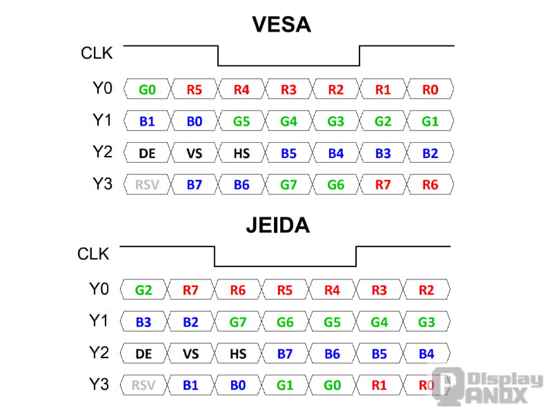
VESA and JEIDA LVDS bit-mapping differences
VESA and JEIDA mappings place the RGB bits in different positions within the serialized LVDS stream. The connector, lane count and clock can all appear correct while the displayed colors remain badly distorted.
The TI RGB-to-LVDS mapping guide documents both formats and shows how single-pixel and dual-pixel data are arranged. It also demonstrates why 6-bit and 8-bit settings cannot be chosen from the connector appearance.
Dual-channel panels introduce another variable: the first pixel may be defined as odd or even by different manufacturers. Swapping the two channels can correct one panel and break another. The panel’s own mapping table must settle the assignment.
Connector Pin Count Is Not a Standard
Two LCD panels may both use a 30-pin or 40-pin connector while having different interfaces, voltages and pin assignments. Some 30-pin panels use LVDS; others use eDP. A cable designed for one model should not be assumed compatible with another model.
The full panel model number is considerably more useful than screen size or connector count when selecting an HDMI to LVDS converter board.
Common HDMI-to-LVDS Display Problems
The backlight turns on, but no image appears
Backlight power and LCD pixel data are separate paths. This symptom commonly points to an incorrect LVDS cable, disabled panel power, wrong firmware, incompatible timing or a single-channel/dual-channel mismatch. A black image caused by unsupported HDCP content is also possible.
The source detects a monitor, but the panel remains blank
Successful HDMI detection only confirms that HPD and EDID communication are working. It does not prove that the advertised HDMI mode can be converted into the required panel timing. The EDID, scaler configuration and LVDS output should be checked together.
Colors are wrong or heavily posterized
VESA/JEIDA mapping and 6-bit/8-bit configuration are the first areas to examine. Incorrect lane order or missing least-significant color bits can produce unusual colors, gradients and vertical artifacts.
The image is divided, duplicated or interleaved
This behavior is strongly associated with an incorrect channel count or reversed odd/even pixel assignment. A dual-channel panel cannot be treated as a single-channel panel simply because a connector can be attached.
The image flickers or disappears at higher resolutions
The output may be exceeding the LVDS transmitter’s pixel-clock range, or the differential routing may have insufficient signal integrity. Cable length, pair impedance, pair-to-pair skew, power noise and connector quality become increasingly important as the lane rate rises.
The controller repeatedly restarts
An undersized power supply or overloaded backlight driver can cause voltage collapse when the panel starts. Panel logic power, backlight power and the controller’s own consumption should be included in the supply calculation.
FPGA-Based HDMI-to-LVDS Conversion
An FPGA implementation is useful when a fixed-function controller cannot provide the required timing or video processing. The supplied engineering material demonstrates an architecture in which HDMI is decoded into RGB data, synchronization signals and pixel clock information before being reordered and serialized for LVDS output.
On Xilinx 7-series devices, OSERDESE2 resources can perform high-speed parallel-to-serial conversion, while differential output buffers drive the LVDS pairs. AMD’s OSERDESE2 application documentation confirms the use of these resources for high-speed LVDS interfaces.
FPGA logic can also add test patterns, image processing, pixel reordering, source selection, OSD composition or custom output timing. HDMI reception may be implemented in programmable logic for suitable data rates or handled by an external HDMI receiver that outputs parallel RGB.
The flexibility comes with additional work. Clock-domain crossing, timing closure, differential routing, EDID, HDMI equalization, HDCP requirements and panel power sequencing still have to be engineered. For a conventional LCD monitor, a dedicated bridge or scaler SoC is usually more economical. FPGA becomes attractive when its programmable video path solves a requirement that a standard board cannot.
Typical Applications
HDMI to LVDS converters remain useful wherever an established LVDS LCD panel must operate with a modern HDMI source. Common applications include industrial HMIs, test instruments, medical equipment, inspection systems, kiosks, digital signage, custom monitors and panel evaluation fixtures.
They are also used to maintain equipment built around discontinued controller boards. Replacing the signal-processing board can extend the service life of a qualified LCD panel without redesigning the complete mechanical assembly.
For production equipment, long-term component availability, operating temperature, EMC performance, startup behavior and firmware control normally matter more than the lowest board price.
When a Custom HDMI-to-LVDS Controller Board Makes Sense
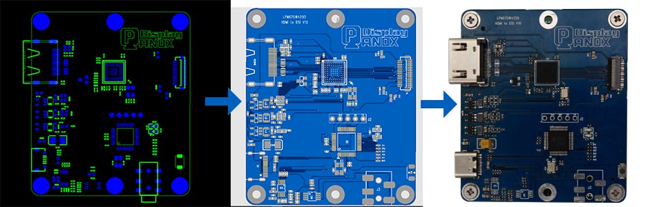
Custom display controller board developed by Panox Display
An off-the-shelf controller is practical when its firmware, cable and power configuration already match the selected panel. A custom solution becomes more appropriate when the project requires a specific PCB shape, connector position, input voltage, boot logo, EDID, OSD, audio output, touch interface, backlight curve or industrial operating range.
Panox Display provides custom HDMI-to-LVDS controller and driver board solutions together with panel-specific cables and firmware configuration. Accurate matching begins with the complete LCD model and panel specification, followed by the required HDMI input modes, native output timing, power source, backlight parameters, touch or audio functions, mechanical limits and operating environment.
This panel-first approach reduces the risk of receiving a board that accepts HDMI but cannot safely drive the intended display.
Conclusion
An HDMI to LVDS converter is a complete display interface subsystem rather than a simple adapter. It has to manage HDMI reception, EDID, video timing, color mapping, LVDS serialization, panel power and backlight control.
Reliable selection begins with the LCD panel specification. Native timing, channel count, color depth, VESA or JEIDA mapping, connector pinout, logic voltage and backlight requirements must all match the board. When these parameters are confirmed together, an HDMI source can drive an LVDS LCD panel with stable timing, correct color and predictable startup behavior.
Learn more: MIPI vs LVDS: Display Interface Differences and Selection Guide
Frequently Asked Questions
Can HDMI be connected directly to an LVDS LCD panel?
No. HDMI and panel LVDS use different signaling formats and control methods. An active bridge, controller board or FPGA-based conversion system is required.
Is an HDMI to LVDS adapter just a cable?
No. Products described as adapters usually contain an HDMI receiver, video processor or bridge IC, LVDS transmitter, firmware and power circuitry. A passive cable cannot decode HDMI and generate panel LVDS timing.
Can any 30-pin HDMI-to-LVDS board drive any 30-pin panel?
No. Pin count does not define the interface, voltage, lane arrangement or mapping. The board, cable and firmware must be matched to the exact panel model.
Does an HDMI to LVDS converter support audio?
The LVDS panel output does not normally carry HDMI audio. Some controller boards extract audio and provide a separate amplifier, headphone connection, I²S interface or S/PDIF output.
Does conversion add display latency?
A direct bridge can have a short processing path because it mainly receives, maps and serializes the video. A scaler-based controller may add more latency due to buffering and image processing. The actual delay depends on the chipset and operating mode and should be measured in latency-sensitive equipment.
Is HDMI to LVDS the same as LVDS to HDMI?
No. The conversion direction is different. An HDMI-to-LVDS board drives an LVDS panel from an HDMI source. An LVDS-to-HDMI board receives an existing LVDS stream and converts it into an external HDMI output. The two designs are not interchangeable.