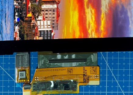
Standard COF OLED 7.8 inch Flexible OLED
Some clients asked for an introduction about COF, so today I will present this to our readers.
Before the adoption of COP packaging technology, COF was considered as the benchmark for "high-end display products." COF packaging technology is known for achieving "narrow bezels," but its "high cost" makes people hesitate.
Therefore, the use of COF packaging technology in certain product areas is controversial, with the debate focusing on: "reducing bezels leads to price increases."
How many consumers are willing to "pay for the price increase caused by reducing the D-Border of display products by 1.X mm" has become a widely discussed topic.
After all, technological innovation, breakthrough, and iteration are achieved through large-scale commercial use, and the benefits generated after commercialization provide feedback. If technological innovation cannot generate commercial value and benefits, it's no different from "being unrealistic."
Speaking of COF, since it involves many aspects, to ensure the quality of the article, today we will mainly focus on COF's structure, classification, and the advantages and disadvantages of different COF structures.
Other aspects, such as COF production process and COF product design points, will be covered in future articles.

COF Structure Analysis and Classification
COF (Chip on Film) is a packaging technology on flexible substrates, which achieves the purpose of reducing product size, enabling free bending, and reducing product bezels by directly packaging the driving IC onto flexible substrates.
When COF is applied to display panels, it can effectively reduce the width of the display panel's D-Border, increase the product's display area ratio, and bring stronger visual impact to consumers.
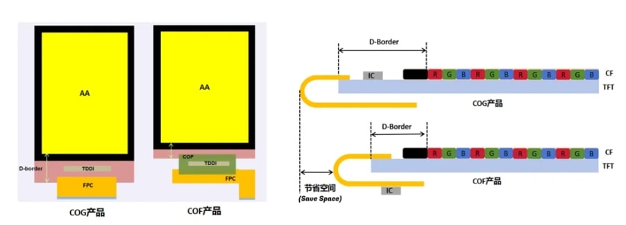
According to state, COF structures can be divided into: roll structure and piece structure; according to the number of layers, they can be divided into: single-layer COF and double-layer COF. Let's explain them one by one.
Roll Structure and Piece Structure
1. Roll Structure
Roll structure consists of many piece structures of COF arranged together. Roll COF cannot be used directly and needs to be punched into single effective COF pieces using molds before use.
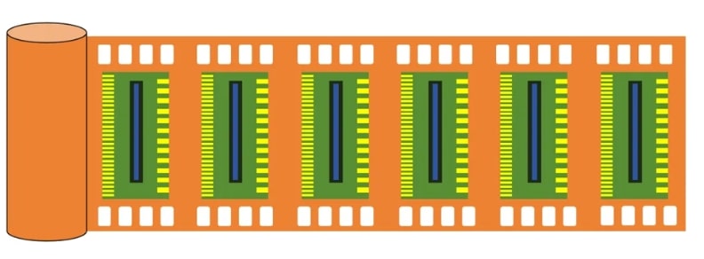
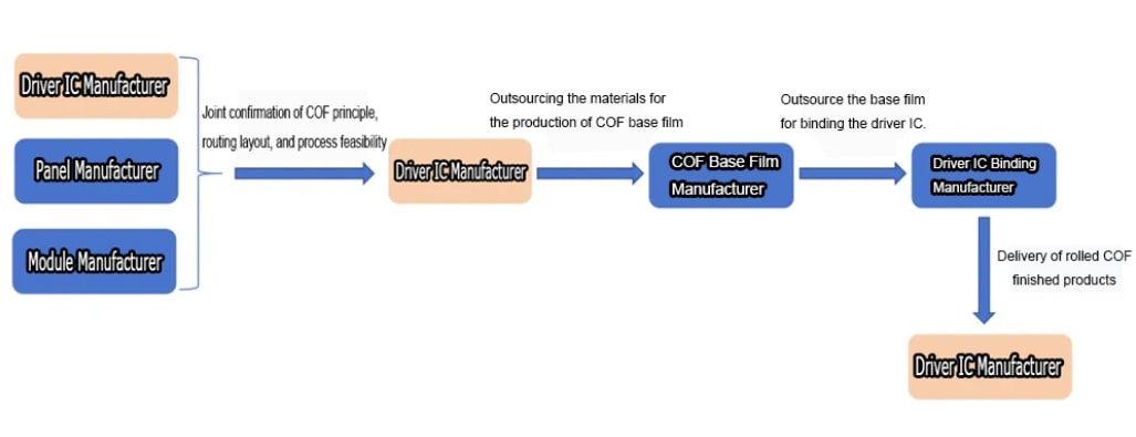
The production process of roll COF is different from other key components of display modules. A complete roll COF product production process involves many suppliers, such as driving IC manufacturers, panel manufacturers, COF flexible base film manufacturers (Base Film), driving IC bonding manufacturers, and module manufacturers.
Generally, the overall process of producing a new COF product is as follows. Of course, due to business model influences, there may be differences between different driving IC manufacturers.
First, the driving IC manufacturer, panel manufacturer, and module manufacturer jointly confirm the COF principle, line layout, and process feasibility; then, the driving IC manufacturer sends the confirmed information to the COF base film manufacturer for production; the produced COF base film is given to the driving IC bonding manufacturer for IC bonding; finally, the roll COF product is delivered to the driving IC manufacturer.
The entire process is led by the driving IC manufacturer as the main body.
2. Piece Structure
The driving IC manufacturer ships the roll COF products to the downstream module manufacturers. The module manufacturer arranges COF punching molds to punch the COF roll material into single effective COF pieces, then binds them with the display panel and FPC/PCB, thus completing a COF display module semi-finished product.

Through the above explanation, you should now have a basic understanding of the process from roll COF to piece COF, and then to COF display module semi-finished products.
So, what is the detailed structure of piece COF?
Piece COF mainly includes: COF base film with CU layer (Base Film, usually made of PI+CU), solder resist green oil, driving IC, and epoxy resin adhesive. The main component materials and their functions are quite easy to understand, similar to FPC.
Simply put, COF is like a high-precision FPC, with conventional COF line width and pitch being about 1/5~1/8 of FPC line width and pitch.
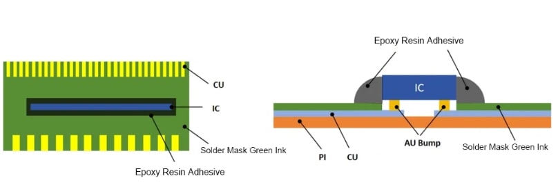
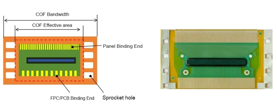
Additionally, there are several key dimensions and positions in piece COF that need special explanation:
a. COF width: Includes the width of the effective COF area and sprocket holes on both sides. Common COF widths used in small and medium-sized display products are mainly 35mm, 48mm, and 70mm, which can be selected according to the number of lines.
b. COF effective area: The effective area that is ultimately used on the product after removing the sprocket holes on both sides, which is also the final shape of the COF.
c. Display Panel bonding end: For COF and display panel bonding end, the bonding finger pitch used on small and medium-sized COF typically ranges from 16~30um, and the bonding finger width is usually between 10~20um. Due to the narrow pitch and width of COF bonding fingers, high precision requirements are placed on bonding equipment.
d. FPC/PCB bonding end: COF to FPC bonding is usually called FOF bonding; COF to PCB bonding is usually called FOB bonding. For COF used in small and medium-sized displays, the FPC bonding end finger pitch is 110~120um, and the bonding finger width is usually 70um, basically consistent with the FPC bonding finger pitch and line width.
e. Sprocket holes: The sprocket holes on both sides of COF mainly serve for positioning, transportation, and process assistance.
Single-layer and Double-layer Structures
Like FPC, COF can be divided into single-layer and double-layer structures. While FPC's single-layer and double-layer structures may not have a significant impact on display panel product structural design, it's different for COF. COF's single-layer and double-layer structures will have significant impacts on display product structural design, material selection, and process flow.

1. Single-layer Structure COF
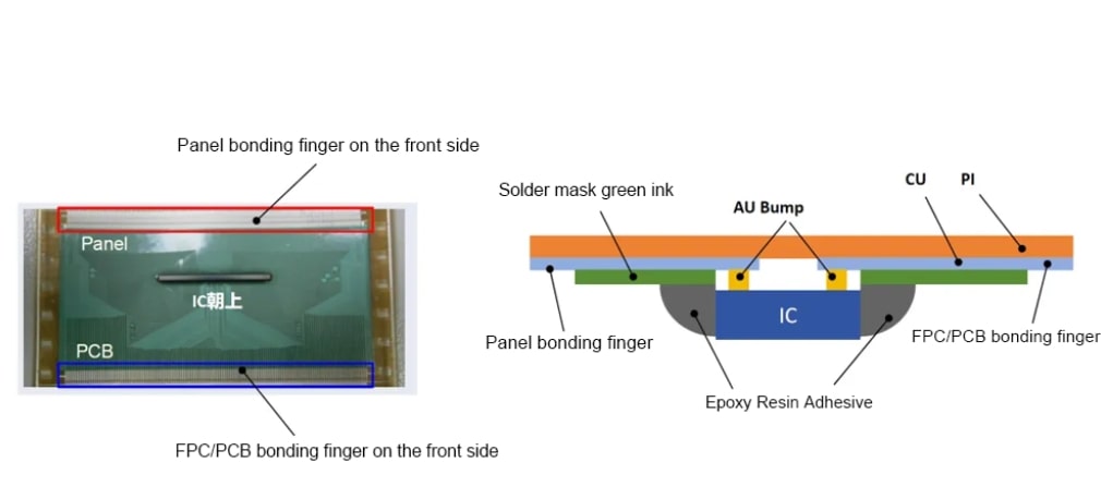
Single-layer structure COF only has one layer of wiring, no vias on the COF, and the panel bonding end, FPC/PCB bonding end, and IC are all on the same side. Currently, most COF used in small and medium display products is single-layer structure COF, mainly due to its obvious price advantage. According to preliminary estimates, single-layer COF is about 5 times cheaper than double-layer COF.
2. Double-layer Structure COF
Double-layer structure COF has two layers of wiring, connecting top and bottom layer wiring through vias, with display panel bonding fingers on one side and IC and FPC/PCB bonding fingers on the other side. Double-layer structure COF has many advantages compared to single-layer structure COF, but its low production capacity and high price are the biggest obstacles to achieving large-scale applications.

Advantages and Disadvantages of Different COF Structures
The impact of using single-layer structure COF and double-layer structure COF on display panel product performance is mainly reflected in IC protection performance, product thickness, product heat dissipation, and product resolution.
1. IC Protection Performance: After double-layer structure COF is folded to the back of the display module, the IC is located on the outside of the display module, visible to the naked eye, and can be clearly identified during the process, which can better avoid IC breakage or cracking caused by human factors.
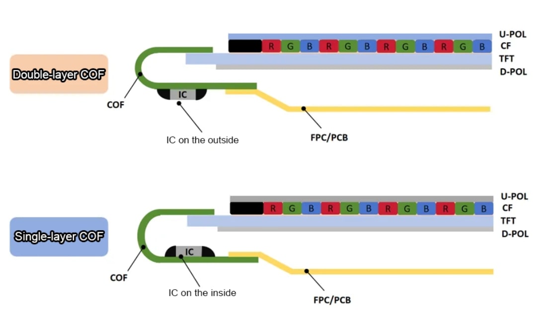
2.Product Thickness: After single-layer structure COF is folded to the back of the display module, the IC is located on the inside of the display module, requiring protective foam padding around the IC, causing the COF bending radius to increase and product thickness to increase accordingly.
For double-layer structure COF, the IC is located on the outside of the display module, requiring no special protection, having a smaller bending radius, and relatively thinner product thickness, which is also more conducive to the overall machine structure design.
3. Product Heat Dissipation: After single-layer structure COF is folded to the back of the display module, the IC is located on the inside of the display module. When the product is powered on, the IC's heat cannot be well released, resulting in poor heat dissipation effect and higher temperature at the display module IC position.
4. Product Resolution: Because double-layer structure COF has two layers of wiring, it can provide more refined circuit design and higher signal transmission quality, enabling higher resolution product applications, such as 2K, 4K resolution display products.
4. Product Resolution: Because double-layer structure COF has two layers of wiring, it can provide more refined circuit design and higher signal transmission quality, enabling higher resolution product applications, such as 2K, 4K resolution display products.


